
Tombstoning—also known as the Manhattan effect or drawbridging—occurs during SMT reflow when a two-terminal passive chip component (such as an 0603, 0402, 0201, or 01005 resistor or capacitor) lifts off one copper land and stands vertically or diagonally on the opposite end. While the final post-reflow defect looks purely mechanical, its trigger is a time-dependent wetting torque imbalance across the component's two terminations during the solid-to-liquid solder transition.
Changing the reflow oven recipe blindly across the whole board before isolating whether the imbalance started in the CAD land pattern, stencil printing (3D SPI), pick-and-place alignment, or local copper thermal mass often shifts defects from one package family to another. For print-stage inspection gates and thermal profiling fundamentals, see our guides on solder paste inspection (SPI) and reflow profile basics.
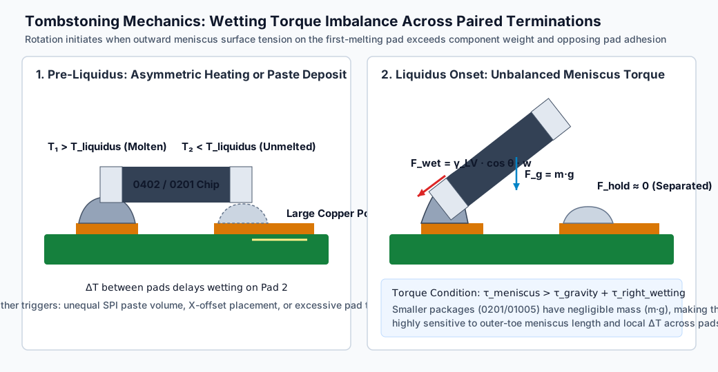
1. The Physics of Tombstoning: Wetting Torque vs. Restoring Forces
When a chip passive enters the reflow liquidus zone, molten solder wets both the PCB copper pad and the component's metallized end cap. Three primary forces act on the component around the pivot edge of the first-wetting pad (Pad 1):
- Downward Restoring Torque from Gravity (τg): The component's weight (Fg = m · g) acts at its center of mass (L/2), pulling the component flat onto both pads.
- Downward Restoring Torque from Opposing Pad Wetting (τhold,2): Surface tension of molten solder underneath the bottom face of Termination 2 pulls that end downward onto Pad 2—but only if Pad 2 has already reached liquidus and wetted the termination.
- Upward Rotating Torque from Outer-Meniscus Wetting (τwet,1): Once solder on Pad 1 melts and climbs up the outer vertical face of Termination 1, surface tension (γLV) pulls outward and upward along the meniscus angle (θ), generating a lifting torque proportional to γLV · \cosθ · w · hterm.
Rotation initiates whenever the outer meniscus torque on the first-melting pad overcomes gravity and any holding force on the second pad:
This equation explains two critical production realities documented in Indium Corporation's tombstoning mechanics analysis:
- Why 0201 and 01005 Passives Are Exponentially More Sensitive: As package dimensions shrink by a factor of k, component mass (m · g) scales with volume (k3), whereas solder surface-tension force scales linearly with termination width (k1). An 0201 or 01005 capacitor has almost zero gravitational restoring torque, meaning even a 0.5--1.5 s difference in melting time between its two ends (τhold,2 ≈ 0) will flip the part upright.
- Why You Cannot Tell Which Pad Melted First from a Post-Reflow Photo Alone: Wait before assuming the lifted end had "too little paste." The standing end is the pad that melted second (or lost contact), while the pivoted end still soldered to the board is the pad that melted and wetted first. However, unequal paste volume, placement skew, or copper heat-sinking can each produce that exact same final posture.
2. Four Engineering Root Causes Behind Wetting Imbalance
A. Thermal Mass Asymmetry (Δ T Across the Two Pads)
If Pad 1 sits on an isolated signal trace while Pad 2 connects directly to a heavy copper ground pour, a power plane, or an un-relieved thermal via, Pad 2 acts as a heat sink during reflow ramp-up. Pad 1 crosses the alloy liquidus temperature (217--220°C for SAC305) first, its outer meniscus pulls the component upward, and Pad 2 is still a solid paste brick with zero wetting hold. The same thermal lag occurs when small passives are oriented parallel to the conveyor travel direction and enter a steep heating zone one termination ahead of the other (Indium Reflow Profile Part II).
B. Land Pattern Geometry and Excessive Pad Toe Extension
When the PCB footprint pads extend too far outward beyond the component body (excessive toe extension), the molten solder meniscus stretches further horizontally, increasing the lifting torque lever arm. Similarly, if the inner gap between pads is too narrow or too wide relative to the component's underside termination width (T), or if one pad is Solder-Mask-Defined (SMD) while the paired pad is Non-Solder-Mask-Defined (NSMD), the wetting geometry becomes inherently unbalanced even when printing and heating are uniform.
C. 3D SPI Paste Volume and Registration Offset
A stencil aperture blockage on one pad—or a global X/Y print registration offset along the length axis of the chip—creates two simultaneous imbalances:
- One pad receives a taller or wider paste brick than its mate, changing local thermal mass and flux capacity.
- Print offset shifts Paste Brick 1 outward toward the pad toe (maximizing lifting torque) while shifting Paste Brick 2 inward toward the gap (reducing contact with Termination 2).
D. Placement Skew, Component Termination Tolerance, and Nitrogen (N2) Effects
If pick-and-place nozzle wear or vision teaching places the chip skewed or shifted toward Pad 1, Termination 2 may barely touch its paste deposit. In addition, while nitrogen (N2) reflow atmospheres improve solderability on oxidized surfaces, introducing high-purity N2 when a thermal Δ T exists between pads can actually worsen tombstoning: reduced surface oxidation increases surface-tension wetting speed (γLV \cosθ) on whichever pad melts first, snapping the component upright before the cooler pad reaches liquidus.
3. Stage-Gated Diagnostic Workflow and Worked Troubleshooting Case
Before touching the rework iron or altering oven zone temperatures, preserve the failed assemblies, record the exact reference designators, panel positions, and component orientations (0°, 90°, 180°, 270°), and classify defects strictly (do not merge vertical tombstones, flat rotational skew / "billboarding", and open solder joints into a single defect bucket).
Use our 8-stage diagnostic matrix (02-tombstoning-diagnostic.csv) to branch by hard process evidence:
| Inspection Stage | Observed Evidence Pattern | Primary Mechanism Hypothesis | Targeted Corrective Action | Mandatory Counter-Check Before Release |
|---|---|---|---|---|
| 1. Pre-Reflow (3D SPI) | One pad consistently prints <75% volume vs. >95% on paired pad | Unequal paste volume delays wetting on low-volume end | Clean stencil underside; inspect aperture walls; adjust aperture area ratio (≥ 0.66) | Verify adequate heel/toe fillet on both terminals and zero bridging on neighboring pitch |
| 2. Pre-Reflow (3D SPI) | Consistent X/Y print offset along component axis across panel | Paste shifted to outer toe of Pad A and inner edge of Pad B | Recalibrate printer fiducial alignment, squeegee stroke offset, and board support pins | Re-verify registration across all four panel corners on 5 consecutive prints |
| 3. Post-Placement (AOI) | Component skewed or overhanging one pad before entering oven | Nozzle vacuum wear, package thickness entry error, or vision offset | Update package library dimensions; check nozzle planarity; center placement over printed paste | Confirm placement Cpk across all 0201/0402 orientations |
| 4. Reflow Ramp / Soak | Tombstoning clusters along conveyor axis or near heavy copper shields | Thermal Δ T across terminations at liquidus entry | Add or lengthen thermal soak plateau (150--180°C for 60--90 s) and slow ramp-to-peak | Confirm extended soak does not exhaust flux activity or induce graping on tiny deposits |
| 5. CAD Copper Review | Pivoted pad is trace-connected; lifted pad connects directly to GND plane | Plane acts as thermal sink delaying liquidus on ground pad | Add spoke thermal reliefs on plane pad in next PCB rev; use inset/home-plate stencil aperture now | Verify thermal-relief spoke width supports required DC current and RF return inductance |
| 6. Footprint Geometry | Pad toe extension >0.35 mm on 0402/0201 or mismatched SMD/NSMD pads | Oversized outer meniscus increases upward pulling vector | Trim stencil aperture outer edge inward by 10--15% (or reduce CAD pad toe in next rev) | Verify terminal wetting still meets IPC-A-610 Class 2/3 minimum end-joint height |
Worked NPI Case: Isolating Recurring Tombstoning at Location R18
During a pilot build containing forty 0402 resistors per board, location R18 tombstones on 6 out of 50 panels, always pivoting upright on Pin 1 (leaving Pin 2 lifted). The remaining thirty-nine 0402 resistors—drawn from the exact same component reel—remain 100% seated. The line technician initially proposes raising the reflow preheat soak temperature by +15°C across the entire oven.
Instead of altering the global thermal profile for a single designator, the NPI engineer pulls the four local records for R18:
Evidence Checked at R18 |
What the Record Shows | Engineering Conclusion |
|---|---|---|
| Defect Population Map | Fails only at R18; 39 other 0402 parts from the same reel have 0 defects |
Rules out a bad component lot or a globally wrong reflow profile |
| CAD Layer / Copper Audit | R18 Pin 1 connects to a 0.15 mm signal trace; Pin 2 connects via a 0.50 mm solid neck directly to a 2 oz GND pour |
Pin 2 has higher thermal mass (heat sink), making Pin 1 melt first |
| 3D SPI Paired Deposit Log | R18 shows a repeatable +0.045 mm X-offset toward Pin 1's outer toe due to a local stencil aperture edit |
Extra paste on Pin 1's outer edge amplifies τwet,1 while Pin 2 lags thermally |
| Pre-Reflow Placement AOI | Component body is centered within ± 0.015 mm of nominal footprint centroid | Pick-and-place machine alignment is not the primary driver |
Controlled Trial & Resolution:
- Immediate Process Fix (Current Lot): Correct the local stencil offset and modify
R18's stencil apertures to an inset / home-plate design (pulling the outer aperture edge inward by 0.05 mm to reduce outer-toe meniscus torque while keeping 85% aperture area over the inner pad region). - Counter-Check: If correcting the print offset and aperture shape eliminates
R18lifting across the next 50-board verification run while maintaining IPC-A-610 fillet compliance, lock the stencil revision. IfR18still lifts despite balanced SPI deposits, add a brief pre-liquidus soak adjustment to close the Δ T caused by the 2 oz GND pour—and log an Engineering Change Request (ECR) to add spoke thermal reliefs toR18Pin 2 in the next PCB layout revision.
4. NPI and Procurement Checklist for Passive-Dense Assemblies
When quoting or transferring an assembly populated with 0402, 0201, or 01005 passives, align the following engineering and quality gates before releasing production:
- Footprint & Stencil DFM Audit: Have the assembler's NPI team verify passive land patterns against IPC-7351 and component manufacturer datasheets, flagging any two-terminal footprints with asymmetric copper pours, via-in-pad proximity, or mixed SMD/NSMD solder-mask openings.
- Paired-Pad 3D SPI Rules: Configure 3D SPI recipes not only for individual pad volume/height limits, but also for paired-pad differential volume and X/Y offset alarms on 0201/0402 components.
- Controlled Trial & Rework Traceability: Require any reworked tombstone boards to be logged by designator and lot prior to touch-up so first-pass yield (FPY) data and root-cause corrective actions remain intact.
- Downloadable Diagnostic Worksheet: Use 02-tombstoning-diagnostic.csv to structure NPI failure analysis and corrective-action sign-off.
HILPCB's SMT assembly lines support 0201 passives as standard and 01005 / 008004 micro-passives by advanced-route review, backed by high-precision placement platforms (±25 µm standard / ±8 µm advanced 3σ reference), 100% inline 3D SPI, multi-zone forced-convection reflow profiling, and 2D/3D AOI. Upload your Gerber, BOM, and CPL files when you request a quote so our assembly engineers can audit your passive footprints and stencil design before first-article production.
Frequently Asked Questions
Which end of a tombstoned component melted first during reflow?
The end that remains soldered down (pivoted) to the PCB pad is the end that melted and wetted first. Once molten solder climbed the outer face of that first termination, surface tension pulled the component upright because the opposite pad (now lifted in the air) had either not yet melted, had insufficient flux/solder contact, or had lost physical contact due to placement skew.
Why can switching to a nitrogen (N2) reflow atmosphere sometimes increase tombstoning?
Nitrogen reduces surface oxides on both the copper pad and component termination, which lowers the wetting contact angle (θ) and increases both wetting force and wetting speed. If a thermal imbalance (Δ T) already exists between the two pads, nitrogen causes the hotter pad to wet even more rapidly and aggressively before the cooler pad reaches liquidus, increasing the net lifting torque.
How does a "home-plate" or inset stencil aperture help prevent tombstoning?
Lifting torque is driven primarily by the solder meniscus pulling outward at the outer toe edge of the pad. Shaping the stencil aperture like a home plate—or pulling the outer aperture edge 0.03--0.06 mm inward from the outer edge of the copper pad—shifts the printed paste volume toward the inner gap underneath the component body, maximizing downward holding force (τhold) while reducing outward lifting torque (τwet).
Should I always add thermal relief spokes to passive pads connected to ground planes?
For 0603, 0402, 0201, and 01005 passives where one terminal connects to a signal trace and the other connects to a large copper pour, adding thermal relief spokes (or necking the copper connection so both pads share symmetric copper entry widths) prevents the plane from acting as a heat sink during reflow. For RF bypass capacitors or high-current shunts where low parasitic inductance requires a direct copper connection, keep the copper entry symmetric on both pads or use a pre-liquidus reflow soak plateau and tailored stencil apertures.