
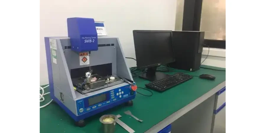
As an instructor at the HILPCB Manufacturing Academy, I’m often asked a core question by design engineers and new process engineers: “My design is theoretically perfect—why does yield still disappoint on the production line?” The answer usually hides in the “gray zone” between design and manufacturing: a complex space defined by process windows, material behavior, and equipment capability. In that space, reflow profile basics is the heart of solder-joint quality and long-term reliability.
This article acts as your virtual production-line guide. In the form of SOPs and checklists, we’ll walk the full journey from a bare board to a functional PCBA. We will focus on how each step influences final soldering outcomes and how HILPCB’s integrated manufacturing-and-test capability helps you build a clear yield improvement roadmap.
Process overview: from design data to finished PCBA
Before diving into details, we need the map. The table below summarizes key pcb fabrication process steps and highlights each stage’s objectives and control parameters. This is not only a manufacturing flow—it is a DFM checklist.
| Process step | Core objective | Key control parameters | Related DFM considerations |
|---|---|---|---|
| 1. Materials & stackup | Establish electrical/mechanical foundations | Laminate Tg/Td/Dk/Df, core/PP thickness, copper weight | Impedance control, stackup symmetry, material selection. See stackup documentation guide. |
| 2. Imaging & etching | Replicate trace geometry accurately | Line/space accuracy, etch factor, undercut control | Min trace/space, copper balance, avoid acid traps |
| 3. Drilling & plated through holes | Build interlayer connectivity | Hole registration, hole-wall roughness, copper thickness | Min drill size, Via-in-Pad, Aspect Ratio |
| 4. Solder mask & legend | Protect copper, prevent mis-soldering | Mask thickness, alignment, hardness | Solder mask dam width, opening accuracy, legend clarity |
| 5. Surface finish | Ensure solderability and oxidation resistance | Plating thickness, flatness, shelf life | Choose OSP/ENIG/HASL, match components and assembly needs |
| 6. SMT assembly | Accurate placement and reliable soldering | Paste volume, placement accuracy, reflow temperature profile | Component spacing, pad design, thermal design (thermal pads, airflow paths) |
| 7. Test & validation | Verify electrical function and reliability | Coverage, false-fail rate, test access | DFT test-point planning, BGA testability, Boundary Scan |
| 8. Cleaning & protection | Improve long-term reliability | Ionic residue, conformal coating thickness/uniformity | Component compatibility, define areas needing local protection |
Control points for imaging/etching and solder mask
The PCB’s “skeleton” is formed here. Tiny deviations can lead to opens, shorts, or impedance mismatch. These often surface only in later electrical tests, but the root cause is here.
Imaging & etching: precision comes first
Imaging uses exposure and development to transfer circuit patterns from film to copper-clad laminate. Etching then removes unwanted copper and leaves the required traces.
- Process window: Etching is chemical; success depends on balancing etchant concentration, temperature, and conveyor speed. The goal is complete copper removal while minimizing lateral attack (undercut) of valid traces.
- Data example: For 35µm (1oz) copper, HILPCB standard etching tolerance can be held within ±12µm, supporting consistent impedance for high-density designs.
- DFM tips:
- Copper balance: Keep copper distribution as uniform as possible across layers to reduce warp/bow caused by uneven etching.
- Avoid sharp corners: Eliminate acute angles that trap etchant and cause over-etching.
Solder mask: the “green armor” of PCBA
Solder mask defines solderable areas and protects non-solder areas from oxidation and short risks.
- Key defect: The most common issue is a solder mask dam that is too narrow or missing, which can create solder bridges (shorts) between adjacent pads during assembly.
- DFM tip: Ensure adequate solder mask dam width between fine-pitch pads (e.g., QFP, BGA). IPC suggests 4mil (100µm) minimum, but HILPCB LDI can achieve 3mil (75µm) dams for more layout headroom in dense designs.
Solder mask SOP checklist
- Registration check: Are solder mask openings precisely aligned to pads? Use AOI for 100% inspection.
- Opening-size check: Do openings meet design requirements—typically 2–3mil expansion per side beyond the pad?
- Surface-quality check: Is the solder mask surface flat, free of bubbles, and free of scratches?
- Cure verification: Use solvent or hardness tests to confirm full cure for mechanical and chemical resistance.
Quality control for drilling, plating, and PTH copper
If traces are the “nerves” of a PCBA, vias are the “synapses” that connect nerve layers. Hole quality directly impacts SI and long-term reliability.
Drilling: mechanical vs. laser
- Mechanical drilling: Used for through holes and blind/buried vias. Wide diameter range and lower cost. Key controls: bit wear and spindle speed to keep hole walls smooth.
- Laser drilling: Used for microvia; a core HDI technology. Very high accuracy but higher cost.
PTH copper: building reliable vertical interconnect
After drilling, the hole wall is non-conductive. Electroless copper plus electroplating forms a uniform copper layer to create interlayer connectivity.
- Quality control:
- PTH copper thickness: IPC-6012 Class 2 requires ≥20µm average. With cross-section analysis and eddy-current test, HILPCB keeps average PTH copper stable above 25µm.
- Hole-wall integrity: Under microsectioning, the wall should show no voids, no nail heading, and no resin recession.
- DFM tip:
- Aspect Ratio: Board thickness divided by minimum hole diameter. Higher Aspect Ratio increases plating difficulty; generally keep within 10:1 for good plating uniformity.
SMT soldering and assembly: the core stage for Reflow Profile
This is where components give life to the PCB, and where reflow profile basics becomes decisive. The SMT flow is a precision chain—every link matters.
Stencil design: where soldering begins
Print quality drives about 80% of solder defects. A solid smt stencil design tutorial will tell you that stencil design is critical.
- Key parameters:
- Thickness: Determines paste volume.
- Aperture design: Aperture shape and size (area ratio / aspect ratio) determine paste release. For 0.4mm-pitch BGA, apertures often include anti-solder-bead features (e.g., “dog-bone” shapes).
- Fabrication method: Laser cutting plus electropolishing significantly improves paste release.
Reflow profile: the soul of soldering
Reflow converts solder paste from a paste into a molten liquid and then cools it into reliable joints. The temperature-time curve is the reflow profile.
Process window: a standard lead-free reflow profile
A typical lead-free reflow profile includes four zones. Each zone has a process window to ensure soldering quality and protect components.
- Preheat:
- Goal: Ramp PCB temperature gradually to activate flux and evaporate solvents, avoiding thermal shock.
- Setting: Ramp rate 1-3°C/s.
- Soak:
- Goal: Equalize temperature across the PCBA, especially between large and small thermal-mass parts.
- Setting: 150-200°C for 60-120s.
- Reflow:
- Goal: Exceed solder-paste melting point (SAC305 ≈ 217°C) to form IMC.
- Setting: Peak 240-250°C, time above 217°C (TAL) 45-90s.
- Cooldown:
- Goal: Cool quickly to form a fine grain structure for best mechanical strength.
- Setting: Cooldown slope -2 to -4°C/s.
Challenge & countermeasure: For PCBAs with very different thermal masses (e.g., heavy copper, large shield cans), a “one-size-fits-all” profile is difficult. HILPCB uses profiler boards with multiple thermocouples to optimize oven settings so every critical point stays within the process window.
Automated inspection: SPI, AOI, and X-Ray
- 3D SPI (solder paste inspection): Before reflow, inspect paste height/volume/area/offset at 100% to eliminate paste-related defects at the source.
- AOI (automated optical inspection): After reflow, detect wrong/missing parts, tombstoning, polarity errors, insufficient solder, and other visible defects.
- X-Ray: For bottom-terminated parts such as BGA and QFN, X-Ray is the only effective way to detect internal voiding, shorts, and opens.
Cleaning, conformal coating, and reliability treatment
After soldering, flux residues remain. For high-reliability products in medical, automotive, or aerospace, residues are a hidden risk.
- Cleaning: Use aqueous or semi-aqueous cleaners; validate results with ion chromatography.
- Data example: Per IPC-J-STD-001, ionic contamination should be below 1.56µg NaCl eq./cm² for high-reliability products.
- Conformal Coating: Apply a thin polymer film to protect the PCBA from humidity, salt fog, and dust—significantly improving lifetime in harsh environments.
Test matrix: ensuring every PCBA is functional
Manufacturing ends where testing begins. A comprehensive strategy is the final safeguard for outgoing quality.
| Test type | Stage | Primary goal | Defects covered | DFT recommendations |
|---|---|---|---|---|
| AOI/X-Ray | Post-assembly | Detect process defects | Solder defects (short/open/insufficient), wrong/missing parts | Break out test points for critical BGA nets to aid X-Ray diagnosis |
| ICT | Post-assembly | Check component values and net connectivity | Wrong values, opens, shorts, IC pin opens | Reserve accessible test points for every net; pitch >1.27mm |
| FCT | Post-assembly / final | Emulate operating conditions and validate function | Functional logic errors, performance gaps, firmware issues | Provide standard interfaces (e.g., JTAG, USB, UART) |
| Reliability tests | Sampling / qualification | Validate long-term stability under extremes | Early failures, latent design/process issues | Consider thermal cycling, vibration, drop, and other stresses in design |
X-Ray inspection checklist (x ray inspection checklist)
- BGA ball alignment: Are balls centered on pads?
- Short check: Any solder bridges between adjacent balls?
- Open / Head-in-Pillow: Are balls fully fused to pads/leads?
- Voiding: Is internal void ratio within acceptable range (typically <25% area)?
- Ball size consistency: Are all balls uniform after reflow?
Quality and traceability: SPC, MES, and continuous improvement
High yield is not accidental—it is systematic management.
- SPC: Monitor key parameters (e.g., reflow peak temperature, SPI paste volume) via Cpk/Ppk to stabilize the process and enable predictive maintenance.
- MES: HILPCB MES is the “brain” of the factory. From incoming components (each reel has a unique barcode) to shipment, every data point is recorded in real time. This allows tracing any PCBA back to its material lot, equipment, operator, and process settings.
- 8D: When quality issues occur, we run a structured 8D loop—from problem definition and root-cause analysis to corrective and preventive actions—closing the loop and continuously driving the
yield improvement roadmap.
From design to delivery, HILPCB is your reliable manufacturing partner
Understanding reflow profile basics and its upstream/downstream processes is the first step toward high-reliability manufacturing. HILPCB combines advanced equipment, a rigorous quality system, and an experienced engineering team to support everything from DFM/DFT reviews to complex process optimization. Our MES ensures full traceability so every product is evidence-backed.
Contact our technical experts to optimize your next projectHILPCB’s integrated manufacturing and test capability
Turning theory into reality takes strong hardware capability and disciplined workflows.
HILPCB core capability snapshot
- Smart warehousing & material control: Temperature/humidity-controlled storage integrated with MES to ensure FIFO and full traceability—preventing oxidation or mix-ups from the source.
- High-precision SMT lines: Industry-leading DEK printers, Siemens/Fuji high-speed placement, and Heller 12-zone reflow ovens—capable of 01005 and 0.35mm-pitch BGA.
- End-to-end quality monitoring: Standard 3D SPI and in-line AOI on each SMT line, plus high-resolution Omron 3D X-Ray for full-coverage soldering inspection.
- One-stop test solutions: ICT, FCT, Burn-in, and environmental reliability tests (thermal, temperature/humidity cycling) so products meet the highest quality bar before shipment.
- Professional engineering support: Process and test engineers engage early with professional DFM/DFT reports to reduce manufacturing and test risk and shorten time to market.
In short, reflow profile basics is far more than a temperature curve—it is the bridge between design intent and physical reality. With a process-driven understanding of the full pcb manufacturing tutorial and with an integrated partner like HILPCB, you can focus more on innovation while we execute the complex process details.
FAQ
Why is a reflow profile more than just a temperature recipe?
Because it is the process window that determines how solder paste activates, wets, flows, and solidifies around real components on a real board. A good profile balances joint quality, component stress, voiding risk, and throughput rather than simply reaching a target peak temperature.
What usually goes wrong when the reflow profile is poorly matched to the assembly?
Teams often see defects such as insufficient wetting, head-in-pillow, tombstoning, excessive voiding, warped components, or long-term reliability weakness. These problems happen because the profile interacts with paste chemistry, board mass, component mix, and oven behavior, so a generic curve rarely works equally well for every assembly.
Why should profile development be linked to design and material decisions?
Because thermal behavior starts long before the board enters the oven. Copper balance, component density, package type, PCB thickness, thermal pads, and laminate choice all influence how heat is absorbed and distributed, so profile tuning works best when it is coordinated with design-for-manufacturing choices instead of treated as a downstream fix.
What should be validated before locking a reflow profile for production?
Teams should validate solder-joint quality, wetting consistency, voiding level, component shift, thermal margins, and repeatability across multiple boards and oven runs. The real objective is not to create one acceptable trial run, but to prove that the same quality window can be held reliably in volume production.
Conclusion
This article uses reflow profile basics to walk through the full flow—from materials and imaging, to solder mask, SMT, and test validation—highlighting manufacturing details, QC checkpoints, and DFM tips. By following the checklists and process windows, and by involving HILPCB’s DFM/DFA team early, you can accelerate prototype and production delivery while maintaining quality and compliance.
If you need manufacturing and assembly support, contact HILPCB Turnkey Assembly or SMT Assembly for DFM/DFT suggestions.