
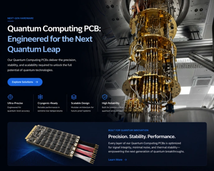
The global quantum computing market reached $1.3 billion in 2024 and is projected to exceed $12 billion by 2032, with IBM, Google, IonQ, Rigetti, Quantinuum, and dozens of startups scaling qubit counts beyond 1,000 and pushing gate fidelities above 99.9%. Quantum computers operate at the intersection of physics and electronics — superconducting qubits function at 15 millikelvin inside dilution refrigerators, trapped ions are manipulated by precision laser and RF systems at ultra-high vacuum, and photonic qubits travel through silicon photonic circuits at room temperature. The Quantum Computing PCB enables all of these modalities by providing the control, readout, and signal conditioning electronics that bridge the quantum processor and the classical computing world.
While the quantum processor operates in exotic conditions, the electronics driving it are built on conventional PCB technology — with extraordinary performance requirements that exceed what most commercial RF or mixed-signal boards demand. Qubit control requires phase-stable microwave signals at 4–8 GHz with <0.5° phase accuracy across hundreds of channels, readout amplifiers must resolve single-photon-level signals at -130 dBm, and the entire control stack must operate with sub-nanosecond timing synchronization across channel counts that double with each processor generation.
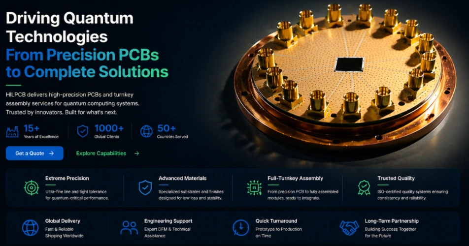
HILPCB manufactures quantum computing PCBs — achieving ±3% impedance control on Rogers 4003C/4350B at 4–12 GHz and >75 dB inter-channel isolation — for quantum hardware companies and research laboratories developing superconducting, trapped-ion, and photonic processors across the United States, Canada, Europe, Japan, and Australia.
Menu Navigation
- The Quantum Electronics Stack: Where PCBs Fit
- Microwave Control Signal Generation at 4–12 GHz
- Single-Photon Readout and Cryogenic Interface Design
- Sub-Nanosecond Timing Distribution Across Hundreds of Channels
- Scaling Control Electronics from 100 to 10,000 Qubits
- Manufacturing Discipline for Quantum-Grade Signal Purity
- Quantum Hardware Programs at HILPCB
The Quantum Electronics Stack: Where PCBs Fit
A quantum computer's electronics span three temperature zones — each placing fundamentally different demands on PCB design, materials, and fabrication. Understanding this architecture is essential because the highest fabrication complexity and commercial volume exist at the room-temperature and 4K interface stages, not at the millikelvin processor level.Room temperature (300K) houses classical control computers, arbitrary waveform generators (AWGs), FPGA-based pulse sequencers, and signal processing platforms. These boards use conventional PCB materials but demand exceptional microwave signal purity, nanosecond timing accuracy, and high channel density — making them the most complex and highest-volume quantum PCB category.
The 4K plate inside the cryostat carries signal conditioning, filtering, and low-noise amplification stages (typically HEMT amplifiers with 2–4 K noise temperature). PCBs at this stage must maintain mechanical integrity and electrical performance at cryogenic temperatures where standard FR-4 becomes brittle, copper conductivity increases 7×, and differential thermal contraction creates mechanical stress on solder joints.
The millikelvin stage (15–20 mK) hosts the quantum processor itself, connected to upper stages through specialty coaxial cables and custom flex circuits. PCB involvement at this stage is limited to specialized interposer substrates and signal routing boards designed for negligible thermal conductivity.
Temperature-Zone PCB Requirements
- Room Temperature Control Electronics: Multi-channel AWG boards (14–16 bit, 10–12 GSPS), FPGA-based sequencers with JESD204B/C interfaces, and RF signal processing platforms requiring microwave purity across 4–12 GHz — boards with 12–20 layers mixing high-speed digital and precision RF on hybrid material stackups.
- 4K Interface Boards: Signal conditioning and filtering stages on materials validated for cryogenic operation — standard FR-4 glass transition occurs at 130–170°C but its mechanical properties degrade severely below -60°C, causing microcracking. PTFE-based and polyimide materials maintain integrity at 4K but require different lamination and drilling processes.
- Cryostat Bulkhead Interface: Hermetic feedthrough boards routing 50–200 coaxial transitions with consistent 50Ω impedance from room-temperature electronics to the cryostat interior — requiring precision connector placement matching the cryostat top plate geometry within ±50 μm.
- Cryogenic Flex Assemblies: Polyimide flex cables using adhesiveless construction with rolled annealed copper — validated through 500+ thermal cycles between 300K and 4K, handling 0.3% thermal contraction per cooling cycle without conductor cracking or impedance shift exceeding ±2%.
Microwave Control Signal Generation at 4–12 GHz
Superconducting qubits are controlled through shaped microwave pulses at frequencies matching the qubit's transition frequency — typically 4–8 GHz for transmon qubits, extending to 12 GHz for fluxonium and other emerging architectures. The control PCB generates, modulates, shapes, and routes these signals from DAC output to the cryostat input port — and any phase noise, amplitude error, or inter-channel crosstalk on the board translates directly to qubit gate errors that limit computational fidelity below the thresholds required for quantum error correction.The relationship between PCB signal quality and quantum gate fidelity is quantifiable: a 1° phase error in a single-qubit π/2 gate produces an infidelity of approximately 1.5×10⁻⁴ — significant when targeting the 99.99% gate fidelity needed for fault-tolerant quantum computing. This means the PCB's phase stability contribution must be held below 0.1° to avoid being the dominant error source.
Microwave Control Board Engineering
- Impedance Precision on RF Laminates: 50Ω microstrip and stripline on Rogers 4003C (Dk 3.38 ±0.05) or Rogers 4350B (Dk 3.48 ±0.05) with ±3% impedance tolerance — significantly tighter than the ±7–10% standard in commercial RF boards. This precision requires SPC-controlled etching with real-time copper thickness monitoring and lamination pressure profiling validated for each material lot.
- Inter-Channel Isolation >75 dB: Ground-fenced stripline routing with via fences at λ/20 spacing (3.75 mm at 8 GHz), individual channel shielding walls at board edges, and optimized SMA-to-stripline launch transitions — preventing crosstalk-induced gate errors when simultaneously driving adjacent qubits during two-qubit gate operations.
- Ultra-Low-Noise Power Distribution: VCO and PLL supply rails with <3 μVrms output ripple (integrated 10 Hz–20 MHz) through cascaded LDO regulators with >60 dB PSRR at 1 MHz. Star-point grounding on dedicated multilayer power planes preventing switching noise from digital sections from corrupting RF local oscillator phase noise performance.
- High-Speed DAC Interface: 14–16 bit DACs operating at 10–12 GSPS with JESD204B/C interfaces routed as matched differential pairs from FPGA to DAC using HDI construction for fine-pitch BGA escape at 0.5 mm ball pitch — with via stub elimination critical for maintaining JESD204C link integrity at 32 Gbaud.
Single-Photon Readout and Cryogenic Interface Design
Quantum processor readout signals are extraordinarily weak — single microwave photons at 4–8 GHz with power levels of approximately -130 dBm (10⁻¹⁶ W). The readout electronics must amplify these signals by 80–100 dB while adding minimal noise — the readout PCB noise floor directly limits qubit state discrimination fidelity and determines whether single-shot readout is achievable versus requiring statistical averaging over hundreds of measurements.The signal-to-noise challenge is extreme: the readout signal power is 10⁻¹⁶ W, while the Johnson noise from a 50Ω load at room temperature is approximately -174 dBm/Hz. The Josephson parametric amplifier (JPA) at millikelvin provides quantum-limited first-stage gain, but the subsequent amplification chain on the readout PCB must not degrade the noise figure by more than 0.5 dB — requiring PCB-level shielding, filtering, and isolation that surpasses what commercial RF receiver designs demand.
Readout System PCB Design
- Shielded Amplifier Chain Layout: Each gain stage in individually shielded compartments with filtered power feedthroughs and absorptive material preventing cavity resonance — noise figure maintained below 1.5 dB through the room-temperature chain through careful grounding topology (star ground at each stage with single-point chassis connection).
- Cryostat Top-Plate Interface Board: 50–200 SMA/SMP/SMPM coaxial-to-PCB transitions with consistent 50Ω impedance (return loss >20 dB to 12 GHz), connector positions matching the physical geometry of the cryostat top plate within ±50 μm. Board materials selected for dimensional stability to prevent connector misalignment during thermal cycling.
- IQ Demodulation Circuit Layout: In-phase and quadrature demodulator circuits with LO-to-RF isolation >55 dB, image rejection >40 dB, and matched I/Q gain and phase balance within 0.1 dB and 1° — enabling single-shot qubit state discrimination with assignment fidelity exceeding 99%.
- Cryogenic Flex Design: Adhesiveless polyimide with rolled annealed copper (RA copper provides 3× better fatigue life than electrodeposited), trace widths calculated for 50Ω impedance accounting for the 7× conductivity increase at 4K that shifts impedance by approximately 3–5%.
Sub-Nanosecond Timing Distribution Across Hundreds of Channels
Quantum gate operations require nanosecond-precision timing across all control and readout channels. A 1,000-qubit processor with multiplexed readout needs 500+ synchronized channels with timing alignment better than 500 ps and trigger jitter below 50 ps RMS — creating a clock distribution challenge that scales quadratically with qubit count as two-qubit gate density increases.Timing errors in quantum systems are not merely performance degradations — they are irreversible decoherence sources. A 100 ps timing misalignment during a two-qubit controlled-Z gate between qubits with 5 GHz transition frequencies introduces a phase error of approximately 0.3 radians — catastrophically degrading gate fidelity. The clock distribution PCB must eliminate this error source by delivering deterministic, matched-delay timing to every channel in the system.
Timing Distribution Board Architecture
- Ultra-Low-Jitter Master Clock: OCXO reference (10 MHz, ±10 ppb) with integrated jitter <50 fs (12 kHz–20 MHz) distributed through impedance-matched 50Ω stripline clock trees on shielded inner layers. Fan-out buffer ICs (LVPECL or CML) with additive jitter <25 fs per stage, with length matching within ±0.5 mil across all destination boards.
- Trigger Synchronization Network: Digital trigger lines from central sequencer FPGA to all channel boards with propagation delay matching within ±50 ps — verified through TDR measurement on production boards. Trigger routing on dedicated signal layers with ground shielding above and below to prevent coupling from adjacent high-speed digital signals.
- High-Speed Data Communication: PCIe Gen 4, 10GbE, or custom LVDS links for waveform upload and measurement data streaming — routed alongside RF signal paths with >60 dB isolation maintained through ground plane continuity and physical separation exceeding 5× trace width.
- Modular Backplane Architecture: Standardized backplane with controlled impedance through all board-to-backplane transitions (via stub length <3 mil through back-drilling), enabling channel count expansion by adding identical daughter boards without re-qualifying the timing distribution network.
Scaling Control Electronics from 100 to 10,000 Qubits
Current quantum computers operate with 50–1,200 qubits, but roadmaps from IBM (100,000 by 2033), Google (1,000,000 by 2029), and others target millions. Control electronics must scale proportionally without proportional cost — the current $500–$1,000 per channel cost of room-temperature control electronics makes a million-qubit system's classical electronics alone a multi-billion-dollar expense at today's architecture.This scaling challenge is fundamentally a PCB architecture problem: increasing channel density per board, reducing per-channel power consumption, and enabling frequency-domain multiplexing that allows one physical line to control multiple qubits. The board architecture choices made for today's 1,000-qubit systems determine whether the electronics can scale to 100,000 qubits through incremental improvement or require complete redesign.
Scalability-Driven Board Architecture
- Channel Density Increase: Moving from 8 to 64 channels per board through higher-integration DAC/ADC ICs, shared LO distribution, and denser RF routing — reducing per-channel electronics cost from ~$800 to <$200 and cutting rack space from 100 to 12 units for a 1,000-qubit control system.
- Multiplexing-Ready Layout: Board layouts accommodating frequency-domain multiplexing (FDM) circuits that assign each qubit a unique readout frequency within a 4–8 GHz band — allowing one physical coaxial line to read out 8–16 qubits simultaneously, reducing cryostat wiring complexity proportionally.
- Cryogenic CMOS Integration Path: Board architectures designed to accommodate future cryogenic CMOS control ICs (operating at 4K) that will move DAC/ADC functions inside the cryostat — requiring new PCB-to-cryogenic-IC interface standards that today's board designs should anticipate.
- Cost Engineering at Scale: DFM optimization, panel utilization maximization, and component standardization across control/readout/timing boards — reducing per-channel electronics cost to the <$50 target that makes million-qubit systems economically feasible.
Manufacturing Discipline for Quantum-Grade Signal Purity
Quantum computing programs span from single-board research prototypes to production systems deployed at quantum cloud providers (IBM Quantum Network, Amazon Braket, Azure Quantum). RF signal quality directly impacts qubit gate fidelity — making manufacturing consistency a scientific requirement with measurable impact on quantum computational results, not merely an engineering quality preference.A 0.2 dB variation in insertion loss between two otherwise identical control channels creates a gate calibration asymmetry that manifests as a systematic error in multi-qubit algorithms. Manufacturing consistency at the level required for quantum hardware demands process control infrastructure that most PCB fabricators reserve for aerospace or defense programs.
Quality Framework for Quantum PCB Programs
- Research Prototypes: 2–10 boards with hand-loaded specialty RF components (coaxial transitions, cavity filters, cryogenic connectors), custom test procedures developed in collaboration with the quantum hardware team, and engineering documentation — delivered in 5–7 working days for rapid hardware iteration during qubit bring-up.
- Production Control Systems: Quantum cloud providers deploying multi-system installations need consistent RF performance across hundreds of identical boards — SMT assembly with SPC monitoring on RF-critical processes (solder paste volume on SMA pads, component placement accuracy on impedance-sensitive traces), 100% AOI, and functional RF test ensures production repeatability.
- RF Performance Verification on Every Board: Network analyzer measurement of insertion loss (±0.15 dB board-to-board), return loss (>20 dB at all frequencies), and inter-channel isolation (>75 dB) on every production board — not sample-based testing. Test results linked to board serial number for correlation analysis with quantum system performance data.
- Full Process Traceability: Laminate lot number, copper foil batch, etching chemistry age, lamination temperature/pressure profile, and all test results linked to each board serial number — enabling root-cause analysis when quantum hardware teams observe performance variations correlated with control electronics changes.
Quantum Hardware Programs at HILPCB
HILPCB manufactures quantum computing PCBs for hardware companies and research laboratories developing next-generation quantum processors — from university groups building their first 10-qubit demonstrator to companies deploying 1,000+ qubit production systems.Our quantum PCB capabilities include high-frequency microwave control boards on Rogers 4003C/4350B with ±3% impedance at 4–12 GHz, HDI construction up to 64 layers for FPGA and DAC BGA escape routing at 0.5 mm pitch, multi-channel readout PCBs with >75 dB inter-channel isolation verified on every board, cryogenic flex cables in adhesiveless polyimide validated through 500+ cycles to 4K, precision clock distribution with <50 fs jitter contribution, and IPC-6012 Class 3 fabrication with RF performance data traceable to individual serial numbers.
Quantum Computing PCB FAQ
Why are standard FR-4 materials unsuitable for cryogenic quantum interfaces?
Standard FR-4 becomes brittle and suffers from severe mechanical degradation (microcracking) at temperatures below -60°C. In the 4K stage of a dilution refrigerator, the extreme thermal contraction requires dimensionally stable materials like PTFE or specialized polyimides to maintain trace integrity and via reliability.
How does PCB phase stability affect quantum gate fidelity?
A phase error as small as 1° on the microwave control board can produce a gate infidelity of 1.5×10⁻⁴, which degrades the capability of quantum error correction. The PCB's phase contribution must be held below 0.1° through precise impedance control and ultra-stable dielectrics.
How is single-photon readout achieved on a PCB without losing the signal?
Readout signals are incredibly weak (~-130 dBm). To prevent Johnson noise or crosstalk from swamping the signal, the PCB uses individually shielded amplifier compartments, star grounding, and multi-stage filtering, ensuring the room-temperature amplification chain adds no more than 0.5-1.5 dB to the noise figure.
Discuss your quantum electronics requirements with our RF engineering team →