
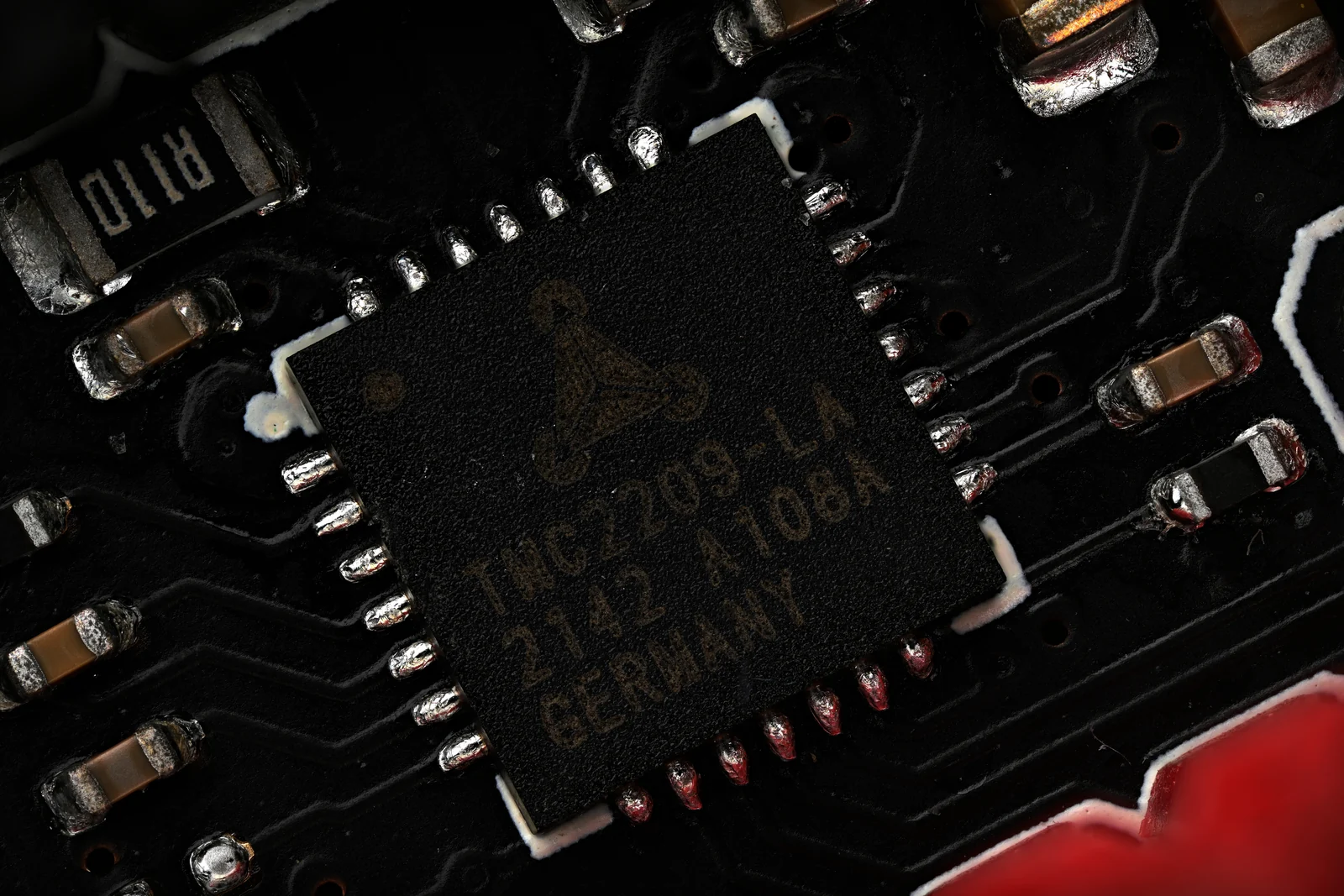
- What goes out of control first on a servo motor driver PCB is usually not the control algorithm, but the lack of clear layout boundaries between the power area, driver area, sensing area, and interface area. Once those boundaries are blurred, false triggering, sensing noise, and EMC variation usually appear together.
- The gate-drive loop has to be laid out according to the real current path. Infineon's gate-driver PCB layout application note explicitly emphasizes building a ground plane, routing VDD and GND close together, and placing the bypass capacitor as close to the gate driver as possible. All of these directly map to the most sensitive parasitic loops on a servo drive board.
- Current-sense layout is not finished just by placing a shunt resistor. TI's current shunt layout material lists three basic rules: place it close to the amplifier, use Kelvin connections, and follow the resistor vendor's layout guidance. That makes it clear that many sensing errors come from the PCB, not from the algorithm.
- For a servo board, EMC starts with return paths and interface-entry control. IEC 61800-3 is the public standards entry point for adjustable speed drive systems EMC, and EMC risk on this type of drive board often starts at the return plane, interface entry, and the boundary between noisy and sensitive areas.
- What is really worth approving is not a board that can spin a motor once, but one that preserves the same drive and sensing window across multiple board builds, loads, and assembly states.
Quick Answer
The core of servo motor driver PCB layout is to freeze power zoning, gate loops, sensing Kelvin paths, interface entry points, and thermo-mechanical constraints first, then optimize details. On industrial motor drive boards, many issues that later look like "software" or "EMC" problems actually originate from these basic layout structures.
Table of Contents
- What should engineers review first on a servo motor driver PCB?
- Summary table of key rules and parameters
- Why must the power area and control area be separated first?
- Why does the gate loop determine switching quality and device stress?
- Why must sensing paths follow Kelvin logic?
- Why should EMC, thermal, and mechanical constraints be frozen together?
- Next steps with HILPCB
- Frequently Asked Questions (FAQ)
- Public references
- Author and review information
What should engineers review first on a servo motor driver PCB?
Start with power zoning, gate-drive loops, current sensing, return paths, interface entries, and thermo-mechanical boundaries.
This does not mean "as long as the MCU and driver IC fit, it is fine," and it does not mean "software filtering and parameter tuning can compensate later." IEC 61800-3 is the public standards entry point for EMC in adjustable speed electrical power drive systems. IEC 61800-5-1 covers electrical, thermal, and energy safety requirements for drive systems. If you look at these public standards together with practical gate-driver and current-shunt layout guidance, the clearest engineering conclusion is that a servo drive PCB must first separate high-noise structures from sensitive structures before talking about algorithm tuning.
Before layout freeze, the five questions that are usually more useful to answer are:
- Have the main power loop, gate drive, sensing, and communication areas already been clearly partitioned?
- Is each gate-drive loop short enough, with a clear return path?
- Is the shunt-to-amplifier connection truly implemented as Kelvin sensing?
- Do encoder, fieldbus, and I/O entries avoid high-noise regions?
- Have hotspots, support points, connector forces, and debug test points already been incorporated into the layout?
If the project has both high current and strong coupling between multiple functional zones, it is usually better to bring the return-plane organization of Multilayer PCB and the current-carrying window of Heavy Copper PCB into the review early, instead of waiting until after the power area is fixed.
Summary table of key rules and parameters
| Rule / Parameter | Recommended range or judgment method | Why it matters | How to verify | What happens if ignored |
|---|---|---|---|---|
| Power zoning | Separate power, driver, sensing, and interface areas first | Reduces coupling and debug difficulty | Layout review, area review | Every problem contaminates the others |
| Gate-drive loop | Keep driver, MOSFET/IGBT, decoupling, and return path as short as possible | Determines ringing, overshoot, and false turn-on | Waveforms, near-field checks, local review | Device stress and EMI increase |
| Sensing layout | Place shunt close to amplifier and use Kelvin connections | Prevents PCB parasitics from introducing large error | Waveforms, offset drift, layout inspection | Current-loop drift and inaccurate protection |
| EMC entry | Keep interfaces, encoders, and communication entries away from noisy areas | Ports are the first places where coupling goes out of control | Pre-scan, entry-area inspection | Repeated EMC rework |
| Thermo-mechanical constraints | Review hotspots, connectors, heatsinks, and support points together | Long-term reliability depends on this | Thermal imaging, vibration/stress evaluation | Solder fatigue, board warp, poor contact |
| Test accessibility | Reserve key waveform and diagnostic points in advance | Both debug and production diagnostics depend on it | Bring-up checklist, fixture review | The issue exists but is hard to localize |
| Public basis | Direct layout implication |
|---|---|
| Infineon gate-driver layout: build a ground plane and keep driver decoupling close to the device | The gate loop must be handled as the shortest return path |
| TI current shunt layout: close to amplifier, Kelvin connection, follow shunt vendor guidance | Current sensing must avoid pulling the inputs into the main current path |
| IEC 61800-3 / 61800-5-1 | EMC, thermal, and safety boundaries cannot be treated separately with optimistic assumptions |
Why must the power area and control area be separated first?
Conclusion: Because the high-noise power paths and low-level control paths on a servo drive board are inherently in conflict, and once zoning is not done first, it is hard to recover later.
On a motor drive board, the main switching loop, gate drive, current sensing, encoder interface, communication port, and MCU area are not just "functional modules." They represent different noise classes and different reference environments. If these areas are not physically separated first, false triggering, sensing drift, communication errors, and EMC variation will follow.
What is more suitable to freeze early is:
- Whether the main power loop is physically separated from the MCU/interface area
- Whether encoder, bus, and low-level measurement areas avoid switching nodes
- Whether isolation boundaries, connectors, and mechanical support points are reviewed together
- Whether the high-voltage boundary is handled according to the real board structure instead of only the schematic abstraction
If the design has already moved into a multilayer board stage, it is usually better to bring real PCB Manufacturing constraints such as interlayer offset, slots, and edge processing into the zoning review instead of judging only from CAD.
Why does the gate loop determine switching quality and device stress?
Conclusion: Because the parasitic inductance inside the gate-drive loop often amplifies overshoot, ringing, and false turn-on faster than the device's own datasheet parameters do.
Infineon's PCB layout guidelines for MOSFET gate driver provides a very direct set of recommendations: build a ground plane, route VDD and GND close together, and place the gate-driver bypass capacitor as close to the device as possible. On a servo drive board, the direct implication is that driver decoupling, output path, and return path must all be as short as possible, and the high-frequency return current cannot be allowed to take a long detour.
The first points worth confirming are:
- Whether the gate driver is too far from the power device
- Whether the local decoupling is attached to the driver, rather than merely being "in the same area"
- Whether the high-side and low-side returns are competing for the same path
- Whether the gate loop crosses or approaches sensitive sensing and communication areas
If the project still needs to inspect local layout expression before the first prototype, it is usually better to review the driver area's traces, vias, and decoupling placement once in Gerber Viewer before moving to fabrication.
Why must sensing paths follow Kelvin logic?
Conclusion: Because on a high-current motor drive board, what often dominates current-sense accuracy is not the amplifier itself, but the PCB layout between the shunt and the amplifier.
TI's current shunt layout material states three rules very clearly: place the shunt close to the current sense amplifier, use Kelvin connections, and follow the resistor vendor's recommendations for footprint and landing pad design. On a servo drive board, that means the high-current main path and the small-signal sensing path must be separated on purpose. The amplifier input cannot simply be tied onto the large current copper.
More reliable handling usually includes:
- Placing the shunt as close to the amplifier as possible instead of routing it over a long distance
- Running separate Kelvin sense lines from both ends of the shunt instead of mixing them into the main current path
- Keeping the positive and negative sensing paths short and symmetrical
- Keeping the key sensing area away from high dv/dt zones and large switched copper areas
If the sensing points need an early structural check, you can also load the related artwork into PCB Viewer for a visual review and confirm that the sense path has not been unintentionally absorbed into the main power copper.
Why should EMC, thermal, and mechanical constraints be frozen together?
Conclusion: Because most field problems on servo drive boards are not purely electrical in the end. They are the combined result of noise, heat, and mechanical stress.
IEC 61800-3 shows that EMC ultimately comes back to system ports and installation state. IEC 61800-5-1 places electrical, thermal, and energy safety inside one framework. For the PCB, this means you cannot leave EMC to the filter, thermal issues to the heatsink, and mechanical issues to the enclosure. Connector force, support points, hotspot distribution, board warp, and interface entry all contribute to long-term stability together.
What should be frozen together includes:
- Whether interface entry points and return paths create new coupling sources
- Whether there is structural stress and solder-joint concentration near hotspot devices
- Whether heatsinks, connectors, and support hardware are pulling the board into local deformation
- Whether test points and debug probe access remain safely reachable
If the project will go through sample validation before volume assembly, it is usually better to bring these checkpoints into a combined review of PCB Prototype and SMT Assembly, instead of waiting until EMC pre-scan or field failures force a layout investigation.
Next steps with HILPCB
If you are working on an industrial servo drive board, BLDC/FOC control board, or another high-dynamic motor drive board, the next step is usually to turn the question from "Can this layout be fabricated?" into "Can the drive and sensing boundaries be reproduced consistently?"
- When the main issues are return planes, power zoning, and high-current windows, first check the fit of Multilayer PCB and Heavy Copper PCB.
- When the gate driver, shunt resistor, and decoupling layout are still evolving, first use Gerber Viewer or PCB Viewer for local review.
- When the project is preparing to validate waveforms, thermal behavior, and assembly state first, moving key structures into PCB Prototype makes it easier to expose issues early.
- When power devices, connectors, and driver areas are about to enter assembly review, bringing in SMT Assembly at the same time is more effective.
- Once layout, validation matrix, and manufacturing notes are frozen, organizing them into Quote / RFQ improves engineering handoff.
Frequently Asked Questions (FAQ)
Which area on a servo drive board tends to fail first?
A: Usually not the controller itself, but the boundaries between power zoning, gate loops, current sensing, and interface entry areas.
Why does gate-driver decoupling have to be placed so close?
A: Because parasitic inductance in the high-frequency drive loop is very sensitive. If decoupling is too far away, the driver's actual supply and return path degrade, and ringing plus overshoot become easier to amplify.
Why must the shunt resistor use Kelvin connections?
A: Because copper, pads, and solder on the high-current path all introduce extra voltage drop. Kelvin connections separate the measurement path from the main current path.
Can EMC issues be solved later by just adding filtering?
A: Not necessarily. If the return plane, interface entry, and high-noise area are fundamentally laid out incorrectly, downstream filtering can usually only provide partial relief.
What is most worth freezing before fabrication?
A: Prioritize zoning, gate-drive loops, sensing Kelvin paths, interface entries, thermo-mechanical constraints, and validation test points.
Public references
IEC 61800-3:2022 | Adjustable speed electrical power drive systems - EMC requirements
Supports the article's explanation that EMC in servo drive systems should be understood from system ports, installation state, and entry control.IEC 61800-5-1:2022 | Safety requirements - Electrical, thermal and energy
Supports the article's statement that thermal, electrical, and energy safety boundaries in drive systems must be considered together at an early stage.PCB layout guidelines for MOSFET gate driver | Infineon
Supports the article's discussion of building a ground plane, routing VDD/GND close together, and placing the gate-driver bypass capacitor as close to the device as possible.Shunt Resistor Layout Considerations | TI Precision Labs
Supports the article's three basic shunt-layout rules: place it close to the amplifier, use Kelvin connections, and follow the resistor vendor's layout guidance.Debugging a Current Shunt Monitor Circuit Layout | TI Precision Labs
Supports the article's note that dedicated Kelvin sense connections are especially important in high-current, low-resistance shunt applications.
Author and review information
- Author: HILPCB Industrial Drive and Control Board Content Team
- Technical review: PCB process, EMC, and assembly engineering team
- Last updated: 2026-05-22