
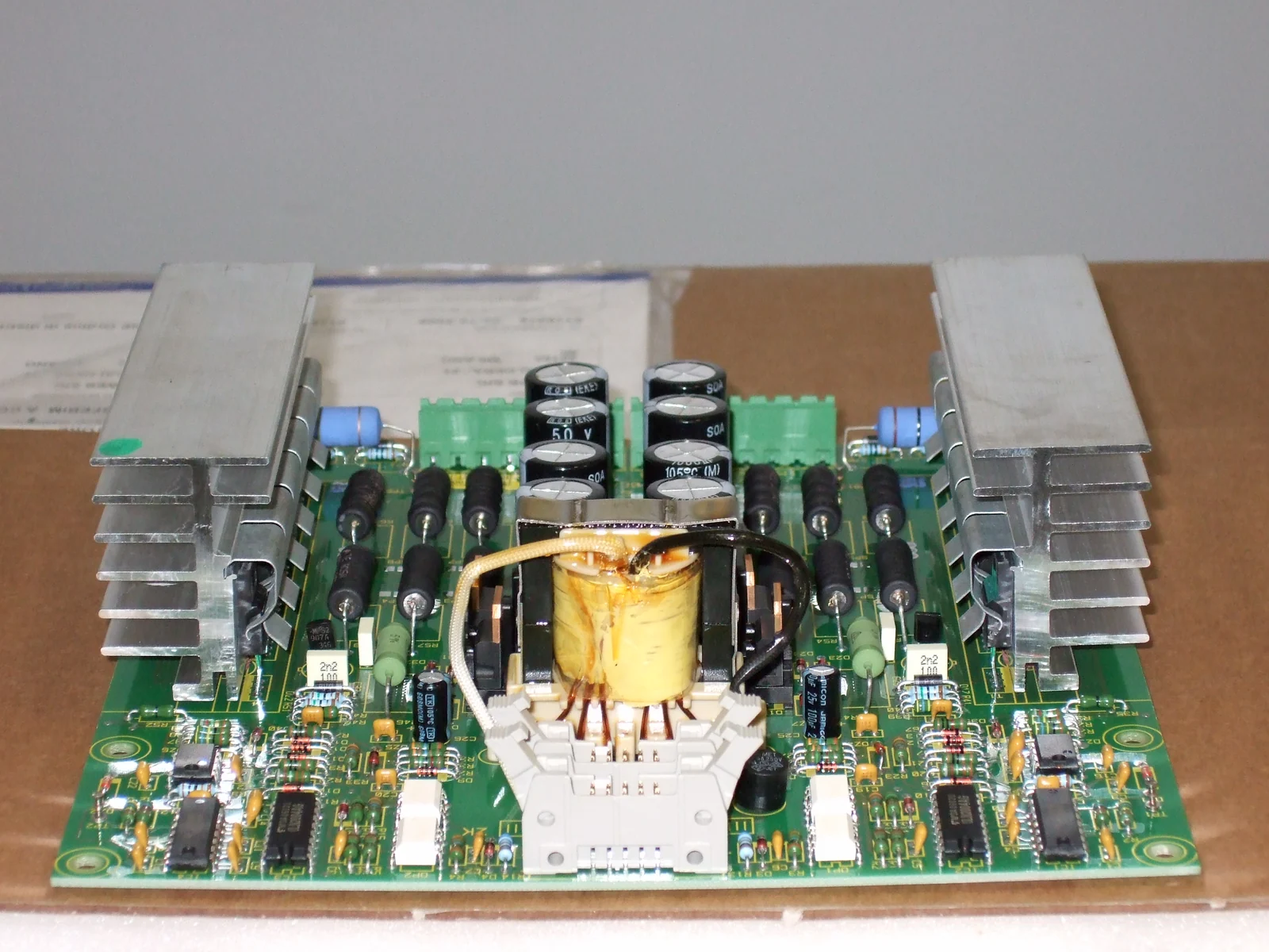
- What is most often underestimated on a three-phase inverter control board is not algorithm complexity, but whether the three drive channels, sensing paths, and interface entry points really form a repeatable physical structure on the PCB. If three-phase layout, return paths, and measurement strategy start from different assumptions, the result keeps showing up later as phase-to-phase mismatch, EMC variation, and slow debugging.
- The gate-drive loop must be handled as a minimum loop. Infineon's published layout guidance for its three-phase inverter evaluation board explicitly says the drive loop should be as small as possible, the VCC and VBS bypass capacitors should stay close to the IC, and the VSS/COM loop should also be minimized.
- The stability of phase-current sensing starts with the shunt and the sense path. The same Infineon document states that the two current-sensing traces should start at the shunt terminals and stay close together. TI's FOC inverter reference designs likewise treat fast current sensing as a board-level structure.
- For an inverter control PCB, EMC is first a return-path problem. The public entry for IEC 61800-3 frames EMC for adjustable-speed drive systems, which means ports, installation state, return planes, and interface entry zones cannot be left until compliance testing to explain.
- A valuable control board is not just one prototype that can drive a three-phase bridge, but one that still gives consistent waveforms and consistent diagnostic access across multiple boards, phases, and lots.
Quick Answer
The core of a three-phase inverter control PCB is making the three gate-drive loops, phase-current sensing, return paths, interface zones, and test points form one symmetrical and verifiable structure. For industrial drives, energy-storage PCS, and renewable inverter boards, protecting three-phase consistency and testability first is usually more effective than trying to compensate later with parameter tuning.
Table of Contents
- What should engineers review first on a three-phase inverter control board?
- Summary table of key rules and parameters
- Why must the noise zone, control zone, and interface zone be separated first?
- Why must gate-drive loops and three-phase consistency be controlled together?
- Why do sensing paths and return paths define the control limit?
- Why can test access, thermal limits, and mechanical constraints not be added later?
- Next steps with HILPCB
- Frequently Asked Questions (FAQ)
- Public references
- Author and review information
What should engineers review first on a three-phase inverter control board?
Start with three-phase zoning, gate-drive loops, phase-current sensing, return paths, interface entry points, and test accessibility.
This does not mean "place the MCU, driver, and connector and the board is basically done," and it does not mean "make one phase work first and then copy it twice." The public IEC 61800-3 context already ties EMC to adjustable-speed electrical power drive systems, while IEC 61800-5-1 addresses electrical, thermal, and energy safety. When those public requirements are combined with Infineon and TI's published three-phase inverter layout guidance, the practical conclusion is direct: a three-phase control board is a combination of symmetrical structure, low-parasitic loops, and verifiable test points rather than a simple extension of a generic control PCB.
Before layout freeze, the five questions that are usually most useful are:
- Whether the three gate-driver areas are structurally consistent and share the same return-path logic
- Whether phase current, DC bus voltage, and fault detection each have a clear sensing path
- Whether the interface zone, encoder zone, and communication zone stay away from high-noise loops
- Whether critical test points are safe to access and sufficient for phase-to-phase comparison
- Whether board bending, connector loading, and local hot spots will break long-term stability
If the project already needs higher current capability, many connectors, or complex control interfaces, it is usually worth bringing the layer-stack return organization of Multilayer PCB together with the current window of Heavy Copper PCB into the control-board review from the start.
Summary table of key rules and parameters
| Rule / Parameter | Recommended range or judgment method | Why it matters | How to verify | What happens if ignored |
|---|---|---|---|---|
| Three-phase zoning | Separate driver, sensing, MCU, and interface regions first | Prevents phase-to-phase and zone-to-zone coupling | Area review, layout review | Three phases behave differently |
| Drive loop | Keep every gate-drive loop small and structurally similar | Controls ringing, overshoot, and phase consistency | Waveform check, local-layout review | One phase is stable, another is not |
| Sensing and return path | Keep shunt-sense routing short, close, and clearly referenced | Determines current-loop accuracy and protection trustworthiness | Waveform, offset, return-path review | Current error and false protection |
| EMC entry zone | Freeze ports, shielding, and return plane early | EMC starts from entry coupling | Pre-scan, entry-zone review | Lab rework cost rises sharply |
| Test accessibility | Reserve comparison test points and fault-injection access | Prototype and production diagnostics depend on it | Bring-up checklist, fixture review | The board works, but cannot be verified efficiently |
| Thermal and mechanical limits | Review connectors, supports, hot spots, and board bend together | Long-term stability depends on them | Thermal image, stress and flatness checks | Solder fatigue and unstable contacts |
| Public layout clue | Direct engineering meaning |
|---|---|
| Infineon 6EDL04I065PR user guide: keep drive loop small, VCC/VBS bypass close to IC | Each phase driver region should be treated as a minimum loop with local decoupling |
| Infineon 6EDL04I065PR user guide: VSS/COM loop connects directly at shunt terminals | Current sensing and power return cannot be separated |
TI TIDA-010023: current sensing with < 1 us settling for 1-, 2-, and 3-shunt FOC inverter |
Sensing path and control speed are directly constrained by board layout |
Why must the noise zone, control zone, and interface zone be separated first?
Conclusion: Because many inverter-control problems are not single-component failures. They are system-level coupling problems caused by unclear boundaries between high-noise and sensitive zones.
Three-phase bridge control boards often carry gate drivers, phase-current sensing, bus sensing, protection logic, encoder or Hall interfaces, communication, and debug links at the same time. If those regions are not separated physically first, high dv/dt switching and large current return will contaminate the control plane along the easiest path.
The items worth freezing early are:
- Whether the three-phase driver region is physically separated from the MCU and interface region
- Whether encoder, CAN/RS485, and debug ports stay away from high-noise zones
- Whether isolation boundaries, connectors, and support points are reviewed together
- Whether high-voltage and interface boundaries are defined from the real board structure instead of only schematic intent
If the project needs denser interlayer transitions or more complex interfaces, it is usually worth bringing the manufacturing limits of PCB Manufacturing into that step rather than leaving those tolerances to the end of the drawing cycle.
Why must gate-drive loops and three-phase consistency be controlled together?
Conclusion: Because on a three-phase inverter, a good single gate-drive loop is not enough. The critical requirement is that all three phases stay as similar as possible structurally.
Infineon's published 6EDL04I065PR evaluation-board guidance gives very direct rules: VCC and VBS bypass capacitors should sit close to the IC, the drive loop should be as small as possible, the VSS/COM loop should also be minimized, and the return should connect directly at the shunt terminals. For a three-phase control board, that means not only making one gate-drive loop short, but also avoiding visible differences between phases in path length, via count, return-plane shape, and decoupling location.
The points worth checking in the same pass are:
- Whether the three gate loops have similar length and similar structure
- Whether local decoupling and bootstrap parts are placed in the same logic position for each phase
- Whether any one phase is squeezed by interfaces or mechanical parts
- Whether structural asymmetry will grow into waveform asymmetry or dead-time tuning burden
When a local structure review is needed, it is usually practical to compare the three driver regions, decoupling, and shunt connections side by side in Gerber Viewer before the asymmetry becomes a hardware problem.
Why do sensing paths and return paths define the control limit?
Conclusion: Because what the controller finally trusts is the measured current, and the measured current depends first on whether shunt, sense trace, and return path are truly clean.
Infineon's inverter-layout guidance states that low-side current-sensing traces should start from the shunt terminals and stay close together. TI's TIDA-010023 places < 1 us settling current sensing directly in the context of 1-shunt, 2-shunt, and 3-shunt FOC inverter design. That shows a simple engineering reality: on a high-dynamic inverter board, sensing layout is part of control bandwidth.
The points worth confirming first are:
- Whether sense traces start directly from the shunt terminals
- Whether positive and negative sense traces are short, close, and symmetrical
- Whether the COM/VSS return closes locally in the shunt region
- Whether the sensing reference region is interrupted by high-frequency return current or plane splitting
If the project is still comparing different sensing options, it is also useful to inspect the critical area in PCB Viewer and confirm that the current path and the sensing path have not been merged into one large copper route.
Why can test access, thermal limits, and mechanical constraints not be added later?
Conclusion: Because what an inverter control board must deliver is not only functionality, but a structure that can be debugged, verified, and diagnosed repeatedly in production.
Many first-board problems are not cases where the design does not work at all. They are cases where safe test points, phase-comparison access, thermal-observation positions, or structural supports are missing, which makes bring-up and production diagnosis slow. IEC 61800-5-1 reminds teams that thermal and energy safety must be considered at the system level. For the PCB, that means connector stress, hot spots, board bend, support points, and test points all have to be planned during layout.
A practical early check usually includes:
- Whether three gate signals, phase current, DC bus, and fault signals all have reachable test points
- Whether large connectors, standoffs, and thermal hardware create local mechanical stress
- Whether hot parts and isolation parts are concentrated too tightly
- Whether fixtures and rework access have been blocked by components or structure
If the project is moving from prototype toward production, it is usually better to define those constraints early together with PCB Prototype and SMT Assembly rather than discovering too late that test and assembly space are missing.
Next steps with HILPCB
If you are currently designing an industrial inverter control board, an energy-storage PCS control board, or another renewable three-phase drive-control board, the next step is usually to turn "layout completed" into "the structure is verifiable, assemblable, and repeatable in production."
- When the main issue is three-phase symmetry, interlayer return, and the main current window, first review the structural fit of Multilayer PCB and Heavy Copper PCB.
- When driver, shunt, and sense traces are still under adjustment, compare the local structures in Gerber Viewer or PCB Viewer.
- When the project needs early validation of waveforms, phase consistency, and test entry points, moving those critical structures into PCB Prototype exposes problems earlier.
- When connectors, isolation parts, and control zones are entering assembly review, bringing SMT Assembly into the same review is usually more effective.
- When layout, validation matrix, and manufacturing instructions are all frozen, organizing them into Quote / RFQ makes the next engineering handoff easier.
Frequently Asked Questions (FAQ)
Why can a three-phase inverter control board not just copy one phase three times?
A: Because board-edge conditions, interface locations, decoupling placement, and return planes easily make the three phases physically different, and that directly appears in waveforms and debugging behavior.
Which part of the gate-drive loop should be shortened first?
A: First shorten the path from driver to power device, the driver decoupling loop to the IC, and the COM/VSS return loop. Those are the most sensitive sections.
Why are phase-current sensing and return path always discussed together?
A: Because even if the sense trace is short, a poor COM/VSS return loop still injects return noise into the measurement, so the controller does not see a clean current value.
Why must test points be reserved during layout?
A: Because three-phase consistency, fault behavior, and waveform validation all depend on reachable test points. Without them, many issues can only be guessed, not proven quickly.
What is most worth freezing before fabrication?
A: Freeze three-phase zoning, gate-drive loops, sensing paths, return paths, interface entry zones, test points, and thermal-mechanical constraints first.
Public references
IEC 61800-3:2022 | Adjustable speed electrical power drive systems - EMC requirements
Supports the article's explanation that EMC on a three-phase inverter control board should be understood from system ports, installation condition, and return-path behavior.IEC 61800-5-1:2022 | Safety requirements - Electrical, thermal and energy
Supports the article's explanation that thermal, mechanical, and energy-safety boundaries should be considered at layout time.EVAL-6EDL04I065PR User Guide | Infineon
Supports the article's discussion that VCC/VBS bypass capacitors should be close to the IC, the drive loop should be minimized, VSS/COM should connect directly at the shunt terminals, and current-sensing traces should start from the shunt terminals and stay close together.TIDA-010023 Reference Design User Guide | TI
Supports the article's statement that current-sensing settling time in 1-shunt, 2-shunt, and 3-shunt FOC inverter designs is closely tied to board-level layout.TIDA-00913 Reference Design | TI
Supports the article's public context around 48V three-phase inverter design and shunt-based in-line motor-phase current sensing.
Author and review information
- Author: HILPCB industrial inverter and control-board content team
- Technical review: PCB process, EMC, and assembly engineering team
- Last updated: 2026-05-24