
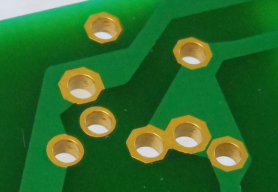
- The first question in VIPPO design is not whether a via can be placed inside a pad, but whether ordinary fanout, ordinary via protection, and the current package pitch can no longer satisfy routing and assembly at the same time. If a simpler fanout still exists, VIPPO is usually not the first answer.
- VIPPO is not one CAD action. It is a combined structure of via protection, via fill, copper cap, pad flatness, and reflow behavior. IPC-4761 is itself a design guide for protection of printed-board via structures, which means via-in-pad has to be specified explicitly rather than guessed by the fabricator.
- On fine-pitch BGA projects, the main risk often appears during assembly rather than during bare-board electrical test. Pad surface state, array coplanarity, and stencil matching often decide yield earlier than whether the drawing merely says "filled via."
- VIPPO is strongly coupled to HDI, microvias, and local copper distribution. IPC has issued public industry warnings on microvia reliability in high-performance products, which means that once via-in-pad is combined with microvias, stacked structures, or multiple reflow cycles, reliability risk has to be moved forward.
- What should really be frozen is a production structure, not just a structure that can be soldered once on a first build. Only when fabrication notes, coupons, cross-sections, X-ray, and post-reflow checks all point to the same definition does VIPPO become production-ready.
Quick Answer
The core of VIPPO PCB design is not pushing a via into the pad by itself. It is proving that via-in-pad really improves breakout, soldering, and thermal path while keeping via fill, copper capping, pad flatness, and reflow behavior repeatable. On fine-pitch BGA and HDI projects, proving necessity first and freezing the structure second is usually the safer path.
Table of Contents
- What should engineers review first in a VIPPO PCB?
- Summary table of key rules and parameters
- When is VIPPO actually the right choice?
- Why must the via-protection definition and filled-via structure be written clearly?
- Why do pad flatness and the assembly window decide production results?
- Why must VIPPO be verified through a reliability loop?
- Next steps with HILPCB
- Frequently Asked Questions (FAQ)
- Public references
- Author and review information
What should engineers review first in a VIPPO PCB?
Start with the adoption reason, via-protection definition, via-fill and copper-cap structure, pad flatness, assembly window, and validation method.
This does not mean "via-in-pad is more advanced," and it does not mean "if the via is filled, it is naturally suitable for a BGA." IPC-4761 is the public design guide for printed-board via protection, and IPC's board-design standards page places it in the same standards context as IPC-2221, IPC-2226, and IPC-6012. For engineering teams, that means VIPPO is not a structure that becomes valid automatically from a layout rule. It has to be clearly specified, manufactured, and validated.
Before layout freeze, the five questions worth answering are usually:
- Whether the current pitch and breakout pressure really force a via-in-pad solution
- Whether solder wicking must be suppressed, or whether breakout paths outside the pad truly need to be shortened
- Whether the via-in-pad region is also coupled to HDI, microvia, or high local heat-flow requirements
- Whether pad flatness, solder-mask definition, and stencil strategy can converge together
- Whether the manufacturing package is explicit enough for both board fabrication and assembly to build the same target structure
If the project has already entered high-density interconnect territory, it is usually better to review the HDI PCB structure window together with the real package array early instead of waiting until BGA fanout is already complete.
Summary table of key rules and parameters
| Rule / Parameter | Recommended range or judgment method | Why it matters | How to verify | What happens if ignored |
|---|---|---|---|---|
| Adoption criteria | Prove that ordinary fanout cannot satisfy density and assembly together | VIPPO is expensive and risky, so the gain must be explicit | Fanout review, package review | Cost and process risk rise without real benefit |
| Via-protection definition | Define via protection, fill, covering, and surface state explicitly | Via-in-pad cannot rely on default interpretation | Fabrication notes, Gerber review | The board shop and assembly team read different structures |
| Pad flatness | Judge array consistency instead of one pad's appearance | It directly affects printing, placement, and reflow | First-article appearance, coplanarity, X-ray | Head-in-pillow, cold joints, and yield drift |
| Structural coupling | Evaluate VIPPO together with microvias, buried vias, and local copper thickness | Stacked structures amplify stress | Cross-section, DFM review, post-reflow checks | The sample is fine, production is not |
| Assembly window | Freeze stencil, paste, solder-mask bridge, and rework limits together | VIPPO risk often appears first in SMT | SMT DOE, first-article review | Bare-board test passes, assembly yield falls |
| Validation loop | Review coupon, cross-section, X-ray, and post-reflow state together | First-board success is not the same as repeatability | Multi-board validation, lot traceability | Latent defects emerge later in the flow |
| Early question | Better engineering action |
|---|---|
| Only local routing is tight | Compare the real gain of dog-bone fanout versus VIPPO first |
| BGA pitch is tight and solder wicking is unacceptable | Freeze integrated pad-plus-via structure and assembly conditions early |
| The project also uses HDI or microvias | Review via-in-pad and microvia structure together instead of deciding separately |
| The team needs a quick check on drawing clarity | Use Gerber Viewer to compare pad, via, and notes first |
When is VIPPO actually the right choice?
Conclusion: VIPPO is worth introducing only when ordinary fanout has already begun to sacrifice routing space, solder control, or thermal path, and simpler structures cannot solve that problem.
Many teams treat VIPPO as a default move on advanced boards. That is usually a mistake. The real gain only appears in a few cases: BGA pitch is very tight, dog-bone fanout clearly compresses routing, solder wicking becomes unacceptable, or the pad has to provide a more direct thermal or layer-transition path. If those conditions are not really present, ordinary fanout is usually easier to fabricate and easier to assemble.
The points worth confirming first are:
- Whether the package array is truly blocked by breakout space
- Whether an ordinary via scheme already makes the pad design unacceptable
- Whether the local thermal path genuinely needs a via inside the pad
- Whether only a few critical packages need VIPPO rather than a whole-board default
If the project is still comparing ordinary multilayer and high-density routes, it is usually better to compare Multilayer PCB and HDI PCB in the same structural review instead of defaulting to the most complex option early.
Why must the via-protection definition and filled-via structure be written clearly?
Conclusion: Because the actual manufacturing result of VIPPO depends heavily on what the design explicitly asks for, not on how a factory usually interprets the job.
That is exactly why IPC-4761 matters. It treats via protection as a design object that must be defined, not as a vague fabrication detail. On a VIPPO structure, fill material, covering method, copper cap, final surface state, and the intended pad function must all lead to one interpretation. Otherwise, the board shop, the assembly house, and the design team may all be imagining different structures.
The items worth writing explicitly into the package usually include:
- Which pads require via-in-pad
- Whether those vias are for breakout, heat transfer, or assembly control
- What the fill, covering, and surface-flatness requirements actually are
- Whether microvias, buried vias, or special stackups are also present
- Which locations need coupons, cross-sections, or extra process verification
If the manufacturing package is still evolving, it is usually worth reviewing the critical BGA and via-in-pad zones in Gerber Viewer first so that the layer expression and fabrication notes do not contradict each other.
Why do pad flatness and the assembly window decide production results?
Conclusion: Because for BGAs, LGAs, and fine-pitch packages, VIPPO must finally behave like a stable pad rather than like a special location that is only theoretically solderable.
Many VIPPO boards look perfectly acceptable during bare-board inspection and only begin to show inconsistent paste release, local array-collapse variation, head-in-pillow defects, or X-ray anomalies once SMT starts. The main issue in those cases is usually not whether the drawing says "filled via." It is whether pad flatness, surface state, solder-mask definition, and stencil strategy actually match the via-in-pad structure.
The items worth freezing together are:
- Consistency across the whole pad array rather than appearance of one pad
- Whether the solder-mask style compresses the real paste window
- Whether the stencil is designed for the real pad surface after VIPPO treatment
- Whether critical BGA regions need targeted X-ray sampling after reflow
When the project moves into assembly review, it is usually better to bring the print, reflow, and inspection boundaries of SMT Assembly into the same review rather than treating VIPPO as only a PCB-fabrication topic. If a prototype build is about to start, it is also useful to expose the key structures early in PCB Prototype.
Why must VIPPO be verified through a reliability loop?
Conclusion: Because the real risk of a via-in-pad structure is often not that it cannot be made at all, but that it can be made and soldered once while still drifting later under reflow, lot change, or stress.
IPC's public industry warning on microvia reliability in high-performance products points to a direct reality: many latent failures do not appear during ordinary bare-board acceptance. They emerge after reflow, ESS, or later field stress. Once VIPPO is coupled with microvias, stacked structures, local thermal stress, or repeated reflow, that reliability logic can no longer be ignored.
A practical release path usually includes:
- Freeze the adoption reason. Prove that VIPPO is necessary rather than default.
- Freeze the manufacturing definition. Pad, via, fill, covering, and surface requirements become one version.
- Freeze assembly input. Stencil, solder mask, X-ray sampling, and reflow observation points are defined together.
- Freeze physical validation. Coupon, cross-section, and key-array checks are bound to the drawing revision.
- Freeze lot traceability. Abnormal pads, abnormal lots, and structure revisions can be traced together.
If the project is already close to introduction, it is usually better to organize those constraints directly into Quote / RFQ inputs instead of writing the rules only after first-board problems appear.
Next steps with HILPCB
If you are currently working on a fine-pitch BGA, LGA, module board, or another dense design sensitive to via-in-pad, the next step is usually to turn "can we use VIPPO?" into "is VIPPO really worth using, and can it be repeated stably?"
- When the main issue is dense breakout and local layer escape, first use the HDI PCB path to converge the structure level.
- When the project is still comparing an ordinary approach and a high-density approach, review Multilayer PCB and the VIPPO option in the same design cycle.
- When risk is concentrated in pad behavior, stencil response, and reflow performance, bring the checkpoints directly into SMT Assembly review.
- When the first need is to confirm that the manufacturing drawing really expresses the via-in-pad structure clearly, check it in Gerber Viewer first.
- When the project is ready to move a critical structure into sample or pilot build, pushing the key checks into PCB Prototype and Quote / RFQ usually exposes risk earlier.
Frequently Asked Questions (FAQ)
Should every BGA board use VIPPO by default?
A: No. VIPPO is worth using only when ordinary fanout is no longer acceptable or when solder control and thermal path have a clear, proven benefit.
Why do VIPPO problems often appear only during SMT?
A: Because the structure ultimately changes the real soldering behavior of the pad. Many risks become visible only during printing, reflow, and X-ray.
Is it enough if the drawing only says "filled via"?
A: No. Via protection, covering method, flatness requirement, validation method, and assembly boundaries also have to be defined.
Why should VIPPO and HDI be reviewed together?
A: Because via-in-pad is often coupled with microvias, local high-density layer transitions, stackup complexity, and multiple reflow cycles. Reviewing them separately misses stress and reliability risk.
What is most worth freezing before fabrication?
A: Freeze the adoption reason, pad/via structure definition, flatness and assembly conditions, physical validation method, and lot traceability first.
Public references
IPC-4761 Design Guide for Protection of Printed Board Via Structures
Supports the article's explanation that VIPPO must be specified explicitly as a via-protection structure rather than treated as a vague fabrication default.IPC Board Design Standards
Supports the article's statement that IPC places IPC-4761, IPC-2221, IPC-2226, IPC-6012, and related documents in one board-design standards context.IPC Releases IPC-6012F, Qualification and Performance Specification for Rigid Printed Boards
Supports the article's explanation that complex interconnect structures, test coupons, and rigid-board performance validation should be moved forward into the design stage.IPC Issues Electronics Industry Warning on Printed Board Microvia Reliability for High Performance Products
Supports the article's discussion that microvia-coupled via-in-pad structures may expose latent failures after reflow or later stress.
Author and review information
- Author: HILPCB HDI and assembly content team
- Technical review: PCB process, DFM, and SMT engineering team
- Last updated: 2026-05-26