
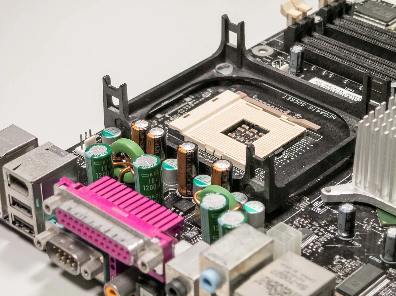
- What goes wrong first on a VRM controller PCB is usually not the controller IC itself, but the fact that the main current loop, feedback sensing, and interphase structure did not converge together in layout. Those issues eventually show up as ripple, overshoot, current-sharing imbalance, thermal drift, and board-to-board variation.
- The first priority in a multiphase VRM is still power-loop geometry, not arranging components around the controller first. TI's multiphase buck design report clearly states that PCB inductance between phases weakens input ripple cancellation. That means the "theoretical advantage" of multiphase power does not automatically hold on the actual board.
- Differential remote sense is not optional polish. It is the key path that keeps point-of-load voltage accurate in a high-current POL design. TI's TPS549B22 and several PMBus buck/controller devices all treat true differential remote sense as a core feature, which means the sensing path itself is part of the power-accuracy structure.
- PMBus telemetry and alarms only matter when board-level behavior is already stable enough. The PMBus specification includes commands such as PAGE, STATUS_WORD, READ_POUT, READ_DUTY_CYCLE, and MFR_SPECIFIC fields. That means monitoring is extensive, but monitoring does not mean the root cause has been removed.
- A VRM layout worth releasing is not one board that can power up, but one that maintains similar transient response and phase distribution across multiple phases, multiple boards, and different thermal states.
Quick Answer
The core of VRM controller PCB layout is to freeze the main current loop, differential remote sense, phase symmetry, thermal spreading paths, and the validation matrix first. In server, ASIC, FPGA, and high-current POL projects, many later problems labeled as "unstable control" or "poor current sharing" actually start from these basic board-level structures not converging together.
Table of Contents
- What should engineers review first on a VRM controller PCB?
- Summary table of key rules and parameters
- Why must layout start from the high-current loop rather than from the controller placement?
- Why must remote sense and the feedback network be laid out from the load point?
- Why does multiphase VRM truly depend on PCB symmetry?
- Why should thermal paths, assembly window, and validation matrix be frozen in the same round?
- Next steps with HILPCB
- Frequently Asked Questions (FAQ)
- Public references
- Author and review information
What should engineers review first on a VRM controller PCB?
Start with the main current loop, differential remote sense, multiphase symmetry, thermal paths, interfaces, and production validation.
This does not mean "as long as the controller supports PMBus and multiphase control, that is enough," and it does not mean "put the controller in the center first and expand the power stage outward." TI's Multiphase Buck Design From Start to Finish clearly points out that as phase count increases, PCB inductance between phases weakens the cancellation of input ripple. The same material also gives a practical rule of thumb: when current per phase rises, cooling, efficiency, and layout cost all require closer evaluation. On a VRM board, that means multiphase power is not a free benefit. It demands tighter layout discipline.
If you then look at devices such as TI's TPS549B22 and TPS53667, you will see that high-current point-of-load power, PMBus telemetry, phase current imbalance detection, and remote sense are all treated as core features. Put together, the most direct engineering conclusion is this: the key to a VRM controller PCB is not how rich the feature list looks, but whether those features are physically realized at the load point, in the loop structure, and along the thermal path.
Before layout freeze, the five questions that are usually most useful are:
- Do the input capacitors, power stage, inductor, and return plane form the minimum main loop?
- Do RSP/RSN or equivalent differential sense lines actually go back to the load point?
- Are the power paths, sense paths, and thermal environment of each phase kept as consistent as possible?
- Are the control area, PMBus area, and high-current area physically separated?
- Does validation cover transient response, current sharing, thermal distribution, and board-to-board consistency?
If the project is a high-current server VRM, FPGA/ASIC POL, or another dense on-board power design, it is usually better to bring the interlayer return structure of Multilayer PCB and the current-carrying boundaries of Heavy Copper PCB into the review early, instead of trying to back-calculate the manufacturing window after the power area has already been laid out.
Summary table of key rules and parameters
| Rule / Parameter | Recommended range or judgment method | Why it matters | How to verify | What happens if ignored |
|---|---|---|---|---|
| Main current loop | Keep input capacitor, power stage, inductor, and return tightly coupled | Determines parasitic inductance, ripple, and overshoot | Waveforms, thermal imaging, layout review | Noise and transient response both degrade |
| Differential remote sense | Route sense lines to the load point and keep them out of switching noise areas | Determines load-point voltage accuracy | Remote load-point measurement, regulation error | The controller sees something different from the real load |
| Multiphase symmetry | Keep path length, copper amount, and thermal environment similar for each phase | Determines current sharing and phase consistency | Per-phase current, thermal imaging, layout review | One phase runs hotter or carries more current |
| PMBus / telemetry | Separate monitoring lines from power lines and do not treat telemetry as a cure | Telemetry only works on top of stable board physics | Status words, power readback, event tracing | Abnormal readings appear, but root cause stays unclear |
| Thermal path | Heat must move into copper, vias, and structural parts | VRM hotspots directly affect lifetime | Thermal imaging, steady-state load, structure review | Long-load drift becomes obvious |
| Assembly window | Review large pads, thick copper, heatsinks, and test points together | Directly affects volume assembly and rework | First article, X-ray, fixture access | Prototype works, but production is unstable |
| Public basis | Direct engineering implication |
|---|---|
| TI SLVA882B: PCB inductance due to phase spacing weakens ripple cancellation | Multiphase layout cannot rely only on "visually even spacing" |
| TI TPS549B22: true differential remote sense amplifier | Load-point sensing must be handled like a protected high-impedance sense structure |
| TI TPS53667: phase current imbalance detection and reporting | Phase inconsistency is a design risk that must be actively monitored and constrained |
| PMBus Part II: commands such as PAGE, STATUS_WORD, READ_POUT, READ_DUTY_CYCLE, PMBUS_REVISION | Digital power monitoring is a complete telemetry and status system, not just a voltage readback |
Why must layout start from the high-current loop rather than from the controller placement?
Conclusion: Because the real determinant of VRM noise floor and transient behavior is the main current loop, not how centrally the controller is placed.
TI's multiphase buck report already explains that phase spacing and board parasitics weaken ideal input-ripple cancellation. The direct meaning for layout is that the input capacitors, power stage, inductor, and return plane have to be arranged around the shortest high-frequency loop, or the board-level benefit gets eaten by parasitics even if the phase count goes up.
What is worth freezing first includes:
- Whether the input ceramic capacitors are placed directly at the power stage and return point
- Whether the SW node area has been compressed enough
- Whether the main power loop avoids unnecessary layer changes and detours
- Whether controller placement is serving the main loop, instead of forcing the main loop to serve the controller
If the project is still comparing local power-stage regions, it is usually better to review the relative placement of input capacitors, the power stage, and the inductor directly in Gerber Viewer rather than judging only from the schematic.
Why must remote sense and the feedback network be laid out from the load point?
Conclusion: Because what a high-current VRM really has to regulate is the voltage at the load point, not some node near the controller that only looks convenient.
The TPS549B22 datasheet lists a true differential remote sense amplifier as a core feature and clearly states that RSP and RSN are high-impedance sense inputs. RSP should connect to the positive sensing point at the load, and RSN should connect to the load return. That means remote sense is not just an ordinary feedback line. It is a high-impedance measurement structure whose reference environment and routing path have to be protected.
What should be confirmed first includes:
- Whether RSP/RSN or equivalent remote sense really returns to the true load point
- Whether the sense lines avoid the SW node, the area under the inductor, and high-current copper paths
- Whether the divider values and routing of the sense network follow the device recommendations
- Whether analog ground is clearly separated from high-current return paths
If the project uses PMBus for margining, telemetry, or fault reporting, this step matters even more, because many "abnormal" readings may actually be caused by layout contaminating the sense path.
Why does multiphase VRM truly depend on PCB symmetry?
Conclusion: Because multiphase current sharing is not ultimately determined by how many phases exist, but by whether the impedance, sensing, and thermal environment seen by each phase are close to the same.
TI's TPS53667 page explicitly lists phase current imbalance detection and reporting as a feature. That alone shows that interphase inconsistency is a real design risk in multiphase VRMs, not an edge case. The controller can detect and report it, but it cannot replace PCB symmetry.
What is better unified during layout includes:
- The path length from each power stage to its inductor, output capacitors, and sense point
- The copper amount and thermal spreading area of each phase
- The decoupling and drive position of each phase
- Whether any phase is forced to deviate because of interfaces, connectors, or structural parts
If the board has to deliver high current while staying compact, it is usually better to use PCB Viewer to compare phase areas and confirm that "nominal symmetry" and real geometric symmetry still match.
Why should thermal paths, assembly window, and validation matrix be frozen in the same round?
Conclusion: Because once a VRM board enters production, electrical, thermal, assembly, and diagnostic issues reveal themselves together, not one by one in sequence.
TI's layout and power-converter materials repeatedly remind designers that power converters are sensitive to both parasitics and heat, while the public description of IPC-A-610 makes clear that it is one of the core standards for assembly acceptance. For a VRM board, that means large pads, thick copper, heatsinks, hold-down hardware, test points, X-ray accessibility, and rework space cannot be treated as afterthoughts.
A more useful validation matrix usually includes:
- Main-loop verification. Review ripple, overshoot, the SW node, and input-loop behavior.
- Remote-sense verification. Compare regulation at the load point with regulation near the controller.
- Interphase consistency verification. Check whether per-phase current, thermal images, and transient response remain close.
- Assembly verification. Check whether thick copper, large pads, and thermal hardware change the soldering window.
- Multi-board verification. Check whether different board builds and different thermal states still produce similar results.
If the project is close to pilot production or NPI, it is usually better to organize these checkpoints directly into the combined inputs for PCB Prototype, SMT Assembly, and Quote / RFQ instead of scattering the validation logic across test records and verbal experience.
Next steps with HILPCB
If you are working on a server VRM, FPGA/ASIC POL, multiphase buck control board, or digital power board, the next step is usually to turn "the schematic is functionally complete" into "the main loop and remote sense can be reproduced stably."
- When the main issues are interlayer returns, high-current copper paths, and the main power region, first check the structural fit of Multilayer PCB and Heavy Copper PCB.
- When interphase layout, input loops, and load-point sensing are still being refined, first use Gerber Viewer or PCB Viewer for local review.
- When the project plans to validate ripple, current sharing, and thermal distribution first, moving the key structures into PCB Prototype makes it easier to expose issues early.
- When thick copper, large pads, heatsinks, and the power stage are about to enter assembly review, bringing in SMT Assembly at the same time is more effective.
- Once the layout, validation matrix, and manufacturing notes are frozen, organizing them into Quote / RFQ improves the next engineering handoff.
Frequently Asked Questions (FAQ)
Is it enough to place the VRM controller in the center first?
A: No. The high-frequency geometric relationship of the main current loop, input capacitor, and power stage usually determines the board's noise floor earlier than controller placement does.
Why must remote sense return all the way to the load point?
A: Because what the VRM truly regulates is the voltage at the load point, not the voltage near the controller. Voltage drop along high-current copper can make those two points significantly different.
If a multiphase layout looks symmetrical, does that guarantee stable current sharing?
A: Not necessarily. What really matters is whether each phase sees a similar path impedance, sense environment, and thermal environment, not just whether the geometry looks visually close.
Can PMBus telemetry solve layout problems?
A: No. PMBus can help expose problems, log status, and track faults, but it cannot replace stable loop design, stable sensing, or stable thermal design.
What is most worth freezing before fabrication?
A: Prioritize the main current loop, load-point remote sense, multiphase symmetry, thermal paths, assembly window, and the validation matrix.
Public references
Multiphase Buck Design From Start to Finish (Part 1) | TI
Supports the article's explanation that PCB inductance in multiphase buck designs weakens ideal ripple cancellation and that phase count plus current per phase must be evaluated together with cooling and layout.TPS549B22 Step-Down Converter With Full Differential Sense and PMBus® datasheet | TI
Supports the article's explanation of the true differential remote sense amplifier, the requirement for RSP/RSN to connect to the load point and return, and the need to protect high-impedance remote sense routing.TPS53667 6-Phase, D-CAP+, Step-Down Buck Controller with PMBus™ | TI
Supports the article's discussion of high-current point-of-load use, phase current imbalance detection and reporting, PMBus telemetry, and remote-sense-related features.PMBus™ Specification, Part II, Version 1.3.1
Supports the article's explanation that PMBus includes telemetry and status commands such as PAGE, STATUS_WORD, READ_POUT, READ_DUTY_CYCLE, and PMBUS_REVISION.IPC Design Standards
Supports the article's point that high-current board design should be understood in the same design context as IPC current-carrying standards such as IPC-2152.Meet Your Standards | IPC-A-610
Supports the article's explanation that IPC-A-610, as an assembly acceptance standard, means the assembly window must be considered together with design.
Author and review information
- Author: HILPCB Power and Server Board Content Team
- Technical review: PI, PCB process, and assembly engineering team
- Last updated: 2026-05-27