At Highleap PCB Factory (HILPCB), we combine multiple inspection technologies—including Automated Optical Inspection (AOI), manual visual checks, In-Circuit Testing (ICT), and advanced X-ray inspection—to ensure complete quality assurance across every layer of the board. X-ray inspection plays a crucial role in detecting hidden solder defects beneath BGAs and within multilayer structures, while optical and electrical tests verify surface accuracy and functionality. This integrated approach ensures our PCB assemblies meet the highest reliability standards in demanding applications.
X-ray PCB Inspection Technology and Working Principles
X-ray inspection technology, also referred to as automated x-ray inspection, is a technology that can find hidden features within a target object. The fundamental principle relies on the differential absorption of X-ray photons as they pass through materials of varying density and thickness. As shown in the above image, the dark black area represents a material made of heavy elements whereas the transparent or comparatively light area represents a material composed of light elements.
Core Components of X-ray PCB Systems:
- X-ray Tube: This tube has the ability to generate x-ray photons and comes in two main types - open tube and closed tube configurations, selected based on required resolution capabilities
- Manipulation Platform: The operation platform moves the sample in different directions, allowing it to be inspected from various angles and magnitudes
- Detection System: The detector on the other side of the sample catches and collects x-ray photons, converting them into an image
The inspection process begins when X-ray photons are generated and directed toward the PCB assembly. The x-ray photons pass through materials differently based on their physical properties, including atomic weight, density and thickness. Solder joints, being composed of heavier elements, appear darker in the resulting images, while lighter materials like PCB substrates and component packaging appear more transparent.
Our multilayer PCB assemblies benefit significantly from X-ray inspection, as this technology can examine internal layer connections and via structures that are completely invisible to optical inspection methods.
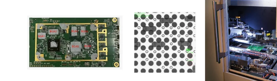
BGA and Hidden Solder Joint Inspection Solutions
Ball Grid Array (BGA) components present unique inspection challenges that make X-ray technology absolutely essential. BGA components are typically tightly encapsulated on the circuit board, leaving almost no space between installed components. This dense arrangement makes it difficult for inspectors to visually identify any defects in the PCB or the mounted components.
Critical BGA Defects Detected by X-ray:
- Missing Solder Balls: Complete absence of solder connections beneath BGA packages
- Solder Bridging: Unwanted connections between adjacent solder balls causing short circuits
- Void Formation: Air pockets within solder joints that compromise mechanical and electrical integrity
- Ball Misalignment: Improper positioning of solder balls relative to PCB pads
PCB X-ray machines are often the best method for evaluating the quality of components and PCB connections, as X-rays can penetrate through BGA components. This non-destructive testing capability allows our quality engineers to assess every solder connection without removing or damaging expensive components.
Beyond BGA inspection, X-ray technology excels at examining other hidden connection types including blind vias, buried vias, and chip-scale packages (CSP). Inspecting these vias visually can be challenging, as they are difficult to detect. PCB X-ray machines emit radiation that can penetrate hidden and hard-to-reach points.
Our SMT assembly processes incorporate inline X-ray inspection to ensure every hidden connection meets our stringent quality standards, preventing field failures and ensuring long-term reliability.
2D vs 3D X-ray Inspection Systems Comparison
Modern X-ray PCB inspection systems offer both 2D and 3D imaging capabilities, each with distinct advantages for different inspection requirements. Understanding when to apply each technology is crucial for optimal quality control results.
2D X-ray Inspection Capabilities: 2D X-ray inspection is a method that utilizes X-rays to create two-dimensional images. This technique involves emitting X-rays from a source, which pass through the object being inspected and are captured by a detector on the opposite side. This approach provides rapid inspection suitable for high-volume production environments.
The primary advantages of 2D systems include faster inspection speeds and lower equipment costs, making them ideal for detecting obvious defects like missing components, gross misalignment, and large solder voids. However, 2D X-ray inspection does not provide depth information or the exact locations of defects, which may hinder the identification of some types of defects.
3D X-ray Inspection Advantages: A 3D x-ray system has the ability to create 3D images of a PCB by building up a series of 2D cross-sections. This is similar to how a CT scan works in the medical industry. Three-dimensional systems utilize computed tomography (CT) or laminography techniques to reconstruct detailed volumetric data.
Laminography serves as a powerful inspection method tailored for flat objects such as integrated circuits, electronic boards (PCBs), and various consumer electronics. Unlike CT scanning, laminography doesn't require full 360-degree rotation, enabling higher resolution imaging with shorter inspection times.
Our advanced inspection capabilities support both high-frequency PCB and ceramic PCB technologies, ensuring comprehensive quality validation regardless of substrate type or application complexity.
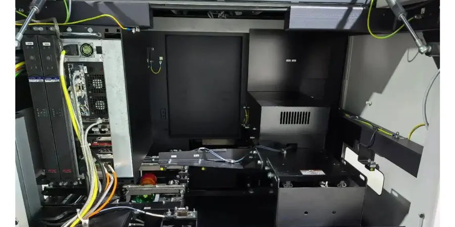
Automated X-ray Inspection Systems and Equipment
Modern automated X-ray inspection (AXI) systems have revolutionized PCB quality control by providing consistent, repeatable results with minimal operator intervention. Automated X-ray inspection (AXI) is the widely used method to determine invisible defects related to ICs (CSP:chip-scale package) and BGAs in printed circuit boards.
Advanced AXI System Features:
- High-Resolution Imaging: Modern systems achieve resolution down to 1 µm for incredibly detailed defect detection
- Variable Magnification: Continuous zoom capabilities from 4X to over 200X optical magnification
- Multi-Angle Viewing: Oblique viewing angles up to 72 degrees for comprehensive solder joint inspection
- Automated Defect Recognition: AI-powered software for consistent defect classification and reporting
The working principle of AXI is similar to that of Automatic Optical Inspection (AOI). The only difference is that AXI uses the X-ray for scanning while AOI uses the light source. This fundamental difference allows AXI systems to detect defects that AOI completely misses, particularly in hidden solder joints and internal component connections.
Our turnkey assembly services integrate inline AXI systems that provide real-time quality feedback during production. This immediate defect detection capability prevents defective assemblies from progressing through subsequent manufacturing stages, reducing overall production costs and improving final product reliability.
The combination of automated inspection with our through-hole assembly capabilities ensures comprehensive quality coverage for both surface-mount and traditional component technologies.
Why Choose HILPCB for PCB Manufacturing and Assembly
Choosing HILPCB means accessing industry-grade inspection at every critical stage of PCB fabrication and assembly. Our facility integrates Automated Optical Inspection (AOI), X-ray inspection, and visual inspection to ensure complete solder joint integrity, component alignment, and solder paste deposition consistency across all production runs.
We apply inline and offline X-ray inspection during surface-mount and through-hole assembly to verify hidden solder connections, especially under BGA, QFN, and CSP components. These non-destructive tests identify solder voids, bridging, and cold joints before final integration, providing confidence for high-reliability applications such as medical devices and automotive electronics.
In addition to X-ray, our inspection ecosystem includes ICT (in-circuit test), functional test, and high-voltage testing, ensuring that every assembled PCB leaves our facility with complete electrical validation. From single prototypes to large-volume assembly, our ISO-certified processes guarantee traceable quality across all PCB types and complexity levels.
X-ray PCB Testing FAQ and Best Practices
How does X-ray inspection differ from optical inspection methods?
PCB X-ray inspection works with the use of X-ray radiation that examines the PCB's internal structure to identify any kinds of defects in the circuit board, while optical inspection only examines surface-visible features. X-ray can penetrate multiple PCB layers and component packages to reveal hidden defects that optical methods cannot detect.
What types of defects can X-ray inspection identify?
X-ray inspection excels at detecting solder joint defects including voids, bridging, insufficient solder, missing components, and connection integrity issues. These images are examined by operators while viewing the inspection monitors to identify open joints, voids, cracks, and shorts. It's particularly effective for BGA, CSP, and other area array package inspection.
What resolution capabilities do modern X-ray systems provide?
Advanced X-ray systems achieve resolution down to 1-2 µm, enabling detailed analysis of the smallest modern components. Generally, for BGAs and CSPs 2 μm resolution is required to provide adequate detail for reliable defect detection.
Can X-ray inspection damage sensitive components?
X-ray inspection is completely non-destructive and does not damage electronic components or PCB materials. The X-ray energy levels used for PCB inspection are far below levels that would cause component degradation or data corruption in memory devices.
How do 2D and 3D X-ray systems compare for different applications?
2D X-ray inspection provides the 2D image of the object. It's like taking a flat picture of the internal structure of a circuit board and offers faster inspection speeds. 3D systems provide volumetric data and better defect localization but require more time and computational resources.
What documentation and traceability do X-ray systems provide?
Modern AXI systems generate comprehensive inspection reports including defect images, statistical analysis, and pass/fail determinations. These reports support quality management systems and regulatory compliance requirements for medical, aerospace, and automotive applications.
How should X-ray inspection be integrated into PCB assembly processes?
X-ray inspection is most effective when integrated at critical process points including post-reflow inspection for surface-mount components and final assembly validation. Inline systems provide immediate feedback for process optimization, while offline systems support detailed failure analysis and process development.