
Ceramic PCB Manufacturer | DBC, DPC and LTCC Substrates
Ceramic PCB manufacturing with Alumina and Aluminum Nitride substrates for power, thermal and RF applications. HilPCB reviews the DBC, DPC or LTCC route, copper, metallization, heat load, CTE, attachment and required thermal or RF evidence before confirming the build.
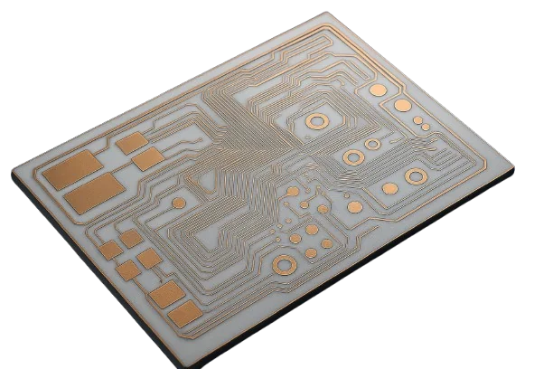
Why Choose Ceramic PCBs
Thermal path efficiency and RF stability in harsh environmentsCeramic substrates provide a direct thermal path from junction to heat sink, enabling reliable operation under high power density and temperature cycling. DBC bonds thick copper to ceramic for low thermal resistance; DPC supports thin-film precision for RF microstrip and coplanar lines. Compared with FR-4, ceramics maintain dielectric stability up to 10–20 GHz with minimal drift in Dk/Df.
Critical Risk: CTE mismatch between die, substrate and package can accelerate solder fatigue and delamination under −55↔+250°C cycling.
Our Solution: AlN (CTE ~4.5 ppm/°C) closely matches silicon, while Alumina provides a cost-effective baseline. We model stress with FEA, validate solder integrity via thermal shock and add design-for-reliability gates such as void limits and bond pull tests. For thermal stack planning, see thermal management notes and RF material selection in high-frequency PCB materials.
- DBC copper for low thermal resistance; DPC for thin-film RF precision
- Stable dielectric properties for RF and microwave designs
- FEA-backed material selection to minimize CTE-induced stress
- Reliability screening: thermal shock, burn-in, bond pull and shear tests
🚀 Quick Quote Request
📋 Get Full Capabilities
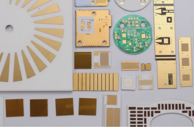
Manufacturing Excellence: DBC, DPC and LTCC
Process control and material traceability for critical applicationsDBC uses high-temperature bonding to attach copper foils to ceramic with bond strength validated by peel tests exceeding 1.4 N/mm. DPC deposits metal via thin-film processes for fine-line control, supporting 50/50 µm trace/space. LTCC cofiring integrates multilayer ceramics with embedded conductors and vias for compact RF modules.
Key parameters are monitored with SPC: copper thickness variation within ±10%, metal adhesion, and via quality. RF performance is verified with TDR and VNA to ensure impedance within ±5% for microstrip/differential pairs. For test strategies and coverage depth, see functional testing.
- DBC bond validation via peel and thermal cycling
- DPC thin-film lines down to 50/50 µm
- LTCC multilayer integration for compact RF modules
- SPC control for copper, adhesion and via integrity
Ceramic PCB Technical Specifications
Material, metallization and test options for power, thermal and RF designs
| Decision Area | Standard Route | Advanced Review | Confirmation Basis |
|---|---|---|---|
Substrate Materials | Alumina (Al2O3) 96% | Aluminum Nitride (AlN), LTCC options | Material datasheets |
Thermal Conductivity | 24–30 W/m·K Alumina | 170–190 W/m·K AlN | Manufacturer specifications |
CTE (Z-axis) | Alumina ~6.5–7.0 ppm/°C | AlN ~4.5 ppm/°C | Material datasheets |
Copper Thickness | 1–2 oz (35–70 µm) | Up to 6 oz | IPC-4562 |
Min Trace/Space | 100/100 µm | 50/50 µm DPC | Process capability |
Operating Temperature | −40°C to +150°C | −55°C to +250°C | Application profile |
Impedance Control | ±10% | ±5% with TDR/VNA correlation | Test methods |
Surface Finish | ENIG, OSP | ENEPIG, Soft/Hard Gold, Wire-bondable finishes | IPC-4552 |
Reliability Tests | Thermal shock, bond pull | Burn-in, high-temperature storage, humidity bias | Customer test plan |
Certifications | ISO 9001, UL, RoHS/REACH | IATF 16949, ISO 13485, IPC Class 3 workmanship | Industry standards |
Need capabilities beyond this product? Explore our full manufacturing capabilities
Ready to start your PCB project?
Whether you need simple prototypes or complex production runs, our advanced manufacturing capabilities ensure excellent quality and reliability. Get your quote within 30 minutes.
Design Considerations: Material, Stackup and Interconnect
Choose AlN when heat flux and CTE matching dominate; choose Alumina for cost-sensitive RF or LED platforms where thermal density is moderate. For extreme heat density or when FR-4 hybridization is required, consider layering with low-loss materials—see Rogers PCB for signal layers while keeping ceramics for the thermal path. When using BeO (Beryllium Oxide) in legacy designs, we handle it under strict safety and compliance controls throughout manufacturing and waste management.
Ceramic substrates win on thermal conductivity and dimensional stability, but they carry a cost and size penalty that not every program can absorb. For designs where the thermal requirement is real but the budget is not ceramic-grade, aluminum and copper core MCPCB construction provides a metal heat path at a fraction of the cost, and the choice between the two is a flux-density decision.
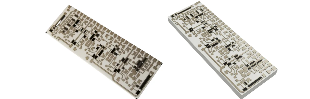
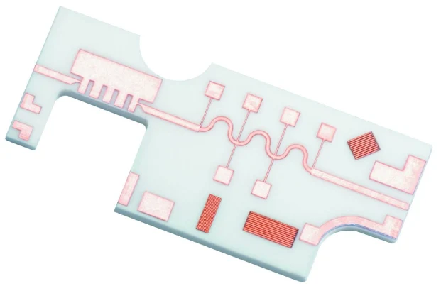
RF and Power Validation
RF structures can be verified with VNA S-parameters and coupon or on-board TDR when included in the quality plan. The RFQ defines the frequency range, fixture, reference plane and impedance limits. Thermal shock, power cycling or burn-in can be added for power modules with an agreed condition, sample plan and failure criterion; see burn-in testing for the questions to resolve.
Ceramic PCB Engineering Examples for Thermal and RF Review
These common engineering scenarios show how HilPCB can review ceramic grade, metallization, attachment, heat flow and acceptance evidence as one released build. The RFQ defines the material, test method, sampling and limits.
Automotive inverter and power modules. Heat flux, isolation voltage, CTE mismatch, copper thickness, substrate flatness and the die or baseplate attachment method determine whether Alumina or AlN and DBC or DPC are appropriate. Use the ceramic substrate selection example to prepare the thermal and mechanical inputs.
Laser diode and high-brightness LED engines. The review connects junction heat, AlN conductivity, copper spreading, solder or sinter attachment, surface finish and mounting flatness. See the AlN ceramic circuit example when defining the heat path and inspection scope.
RF power and microwave front ends. DPC geometry, metallization, ceramic Dk, launch layout and wire-bond finish must align with the electrical model and package. The ceramic circuit manufacturing example organizes the material, fabrication and TDR/VNA questions.
Engineering Assurance & Certifications
Experience: thermal modeling, CTE stress analysis and power-cycling validation can be quoted when the design risk and supplied boundary conditions require them. The method, temperature range, sample plan and failure criteria are agreed before release.
Expertise: engineering reviews DBC or DPC copper, adhesion system, oxide control, flatness, dielectric and insulation requirements against the drawing and attachment method. For process notes, see High-Thermal PCB and Ceramic PCB Design.
Authoritativeness: IPC-6012DS, MIL-PRF-31032, ISO 9001, IATF 16949 or ISO 13485 requirements apply only within the quoted program and applicable certified site.
Trustworthiness: specify the required material CoC, lot reference, calibrated inspection data, thermal or solderability record and traveler retention in the RFQ. HilPCB confirms the included traceability before order release. For related high-reliability platforms, explore High-Thermal PCB.
Ceramic PCB RFQ Requirements
Send the latest Gerber or ODB++ package, mechanical drawing, substrate outline and stackup intent. Identify DBC, DPC or LTCC preference, Alumina or Aluminum Nitride grade and thickness, copper or metallization thickness, finish, via and cavity details, flatness, edge condition, quantities and delivery target.
Add operating and peak temperature, heat source and heat flux, attachment method, CTE constraints, isolation voltage, RF targets, wire-bond or hermetic requirements and acceptance criteria. The 170–190 W/m·K AlN option, 50/50 µm DPC geometry, thick copper and tight flatness are not automatically combinable; engineering confirms the material and process route after review.
Ceramic PCB Testing and Deliverables
Evidence can include material CoC, dimensional and flatness inspection, copper or metallization thickness, adhesion or peel results, dielectric or isolation test, thermal-cycle or thermal-shock data and microsection. TDR or VNA data can be quoted for controlled-impedance or RF structures.
Define the method, fixture, sample plan, temperature range, limits and report format in the RFQ. HilPCB confirms the included evidence before order release so engineering and procurement compare the same acceptance scope.
Frequently Asked Questions
Which ceramic material should I choose for my application?
What documentation is essential for accurate quoting?
How do you verify RF and impedance performance?
Do you support high-reliability packaging features?
Experience Advanced PCB Manufacturing Excellence
From simple prototypes to complex production runs, our world-class factory delivers superior quality, fast turnaround and competitive pricing. Join thousands of satisfied customers who trust us with their PCB manufacturing needs.