
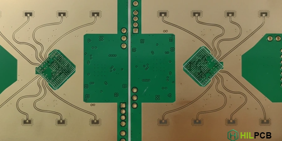
Every trace direction change creates potential for signal degradation at high frequencies. Corners concentrate electromagnetic fields, alter impedance, cause reflections, and can radiate energy. While low-frequency designs tolerate any corner geometry, high frequency routing requires deliberate corner optimization to maintain signal integrity.
This guide provides practical techniques for routing corners in high frequency PCBs, covering the physics of corner behavior and the geometries that minimize degradation.
HILPCB manufactures high frequency PCBs with precise corner geometry control, supporting 45° chamfers, curved traces, and optimized mitered bends for demanding RF and high-speed digital applications.
Why Corners Affect High Frequency Signals
At corners, trace geometry changes abruptly—and at high frequencies, any geometric change affects signal propagation. Understanding corner physics guides proper corner design.
At HILPCB, our DFM review process evaluates corner geometries in high frequency designs to identify potential signal integrity issues.
Impedance Discontinuity
At a right-angle corner, the effective trace width increases where the corner overlaps. This extra copper creates a capacitive discontinuity that lowers local impedance. The impedance dip causes partial signal reflection, creating ringing and reducing signal quality.
For a 90° corner, the effective width increase is approximately 1.4× the trace width. This creates roughly 10-15% impedance reduction at the corner—sufficient to cause measurable reflections at multi-gigahertz frequencies.
Field Concentration
Electromagnetic fields concentrate at the inner edge of corners and spread at the outer edge. This uneven field distribution affects current flow patterns and can increase loss. At very high frequencies (>10 GHz), field concentration at sharp corners can cause radiation.
Propagation Path Length
Signal energy at the inner and outer edges of a corner travels different distances. This path length difference creates small phase shifts between different parts of the signal wavefront—a minor effect in most cases but potentially significant for extremely wide traces or very high frequencies.
Practical Significance
Below about 1 GHz, corner effects are generally negligible for typical trace widths. Between 1-10 GHz, corner optimization improves signal quality and should be applied to critical signals. Above 10 GHz, corner optimization is essential for all high-frequency traces.
90° Corners: The Problem Geometry
Right-angle corners—90° bends—represent the worst case for high frequency routing. They maximize impedance discontinuity and create the sharpest field concentration.
HILPCB recommends avoiding 90° corners on all signals above 1 GHz and on any controlled-impedance traces.
Impedance Effect
The extra copper at a 90° corner creates a capacitive load equivalent to approximately 14% impedance drop. This discontinuity reflects signal energy, with reflection magnitude depending on rise time and corner size.
When 90° Corners Are Acceptable
Despite their reputation, 90° corners cause minimal problems when:
- Signal frequency is below 500 MHz
- Trace is not impedance-controlled
- Rise time is >2 ns
- Corner size is small relative to wavelength
For typical digital signals below 100 MHz, 90° corners are electrically insignificant. The "no 90° corners" rule is often applied too broadly to signals that won't benefit from corner optimization.
When 90° Corners Must Be Avoided
Eliminate 90° corners on:
- RF and microwave traces (any frequency)
- High-speed serial links (>1 Gbps)
- Clock signals (>100 MHz)
- Any controlled-impedance traces
- Differential pairs
Corner Geometry Comparison
45° Corners and Chamfered Bends
Using two 45° bends instead of one 90° bend reduces the corner's electrical impact. This is the most common compromise between routing simplicity and signal integrity.
At HILPCB, our standard fabrication process accurately reproduces 45° chamfer geometries without additional processing requirements.
How 45° Corners Help
Two 45° bends spread the direction change over a longer distance, reducing peak capacitance and field concentration. Each 45° corner adds approximately half the excess capacitance of a 90° corner, but the distributed nature reduces the reflection amplitude.
Effective Impedance Improvement
A properly executed 45° corner reduces impedance discontinuity to approximately 7%—half that of a 90° corner. While still measurable at high frequencies, this improvement is often sufficient for signals up to 5-10 GHz.
Geometric Requirements
For effective 45° corners:
- Segment length between bends should equal or exceed trace width
- Both bends should have equal angles (45° each)
- Maintain consistent trace width through the corner
- Avoid creating notches or bumps in trace edges
Implementation in EDA Tools
Most PCB design tools offer automatic 45° corner options:
- Set routing angle to 45° in tool preferences
- Use chamfer or miter functions on existing 90° corners
- Apply design rules to enforce 45° corners on specific net classes
Mitered and Optimized Corner Geometries
Mitered corners remove excess copper from the corner's outer edge, reducing capacitance and maintaining more consistent impedance through the bend.
HILPCB fabrication processes accurately reproduce mitered corners, including complex multi-segment miters for demanding RF applications.
Optimal Miter Calculation
The optimal miter removes copper to maintain constant impedance. For a 90° corner, the classic miter formula removes a triangle with hypotenuse length of 2× trace width and miter depth of approximately 0.7× trace width.
This "70% miter" reduces impedance discontinuity to approximately 2-3%—acceptable for most applications up to 20 GHz.
Miter Styles
Several miter approaches exist:
- Single chamfer: One diagonal cut across corner (simple, widely supported)
- Double chamfer: Two cuts creating a truncated corner (better impedance)
- Curved miter: Smooth radius replacing sharp corner (optimal but complex)
When to Use Mitered Corners
Mitered corners are appropriate for:
- RF traces above 1 GHz
- High-speed digital above 5 Gbps
- Controlled-impedance traces where 45° corners are insufficient
- Space-constrained areas where curved routing isn't practical
EDA Tool Implementation
Many tools support automatic mitering. Configure miter percentage (70% typical), apply to specific net classes or design rules, and review miter quality in manufacturing output.
Curved Trace Routing
Curved traces—arcs rather than straight segments with bends—provide the smoothest transition and lowest discontinuity. They represent the optimal geometry for demanding high frequency applications.
At HILPCB, our manufacturing processes handle curved traces without issues; curved routing is limited only by EDA tool support and design time.
Why Curves Are Superior
Curved traces eliminate sharp field concentration entirely. The gradual direction change distributes any impedance variation over a longer length, minimizing reflection amplitude. Well-designed curves create impedance variations below 1%.
Minimum Bend Radius
For optimal curved routing, minimum radius of 3× trace width is acceptable, 5× trace width is good, and 10× trace width provides excellent performance. Larger radii are always better electrically but consume more routing space.
Differential Pair Curves
For differential pairs, curved routing maintains consistent spacing throughout the bend. Both traces follow concentric arcs, with the inner trace having a shorter path that requires length compensation. Spacing remains constant at all points, and length matching is achieved through serpentine on the shorter trace.
Practical Implementation
Curved routing requires EDA tool support for arc primitives, more routing planning and manual adjustment, length matching attention for differential pairs, and verification that manufacturing can reproduce curves accurately.
Reserve curved routing for the most critical signals where the performance benefit justifies additional design effort.
Corner Routing for Differential Pairs
Differential pairs present unique corner challenges because both traces must maintain matching while navigating bends.
HILPCB DFM review specifically checks differential pair corner geometry for length matching and symmetry.
Length Mismatch at Corners
At any bend, the inner trace travels a shorter path than the outer trace. This creates skew (length mismatch) that degrades differential signal quality. The mismatch for a 90° corner: ΔL ≈ 0.57 × spacing. For 5-mil spacing, each 90° corner creates approximately 3 mils of mismatch—significant for high-speed signals requiring ±5 mil matching.
Compensation Techniques
Several approaches address corner skew:
- Serpentine on inner trace: Add length after the corner to match
- Alternate inside/outside: Swap which trace is inside at successive corners
- Wider corner radius: Larger radius reduces absolute mismatch
- Corner reflection: Mirror the pair through successive corners
Maintaining Coupling Through Corners
Differential pair coupling should remain constant through corners. Maintain consistent spacing throughout the bend, use symmetric corner geometry for both traces, avoid letting one trace take a tighter radius than the other, and keep both traces on the same layer through corners.
Corner Counting
Track total corner-induced mismatch and compensate at the end of the route. If serpentine is needed, place it immediately after length-mismatching features rather than accumulated at one location.
Related High Frequency Routing Topics
- High Frequency PCB Routing Design: Complete HF routing methodology
- Trace Layout for High Frequency PCB: Geometry optimization strategies
- Routing Clearance in HF PCB: Spacing rules for crosstalk control
- Trace Length Control in HF PCB: Length matching and delay management
- Routing Discontinuity in HF PCB: Managing impedance transitions
HILPCB Corner Routing Services
HILPCB delivers the manufacturing precision your optimized corner geometries require:
Geometry Accuracy: Precise reproduction of 45° chamfers, mitered corners, and curved traces without geometric distortion.
Design Review: Pre-manufacturing evaluation of corner geometries on high-frequency signals with optimization recommendations.
Process Control: Consistent corner reproduction across production lots through controlled etching processes.
Differential Pair Verification: Length matching validation for differential pairs including corner-induced skew assessment.
From prototypes through production, HILPCB maintains corner geometry integrity for high frequency applications.
Contact HILPCB for corner routing review and manufacturing quotation.