
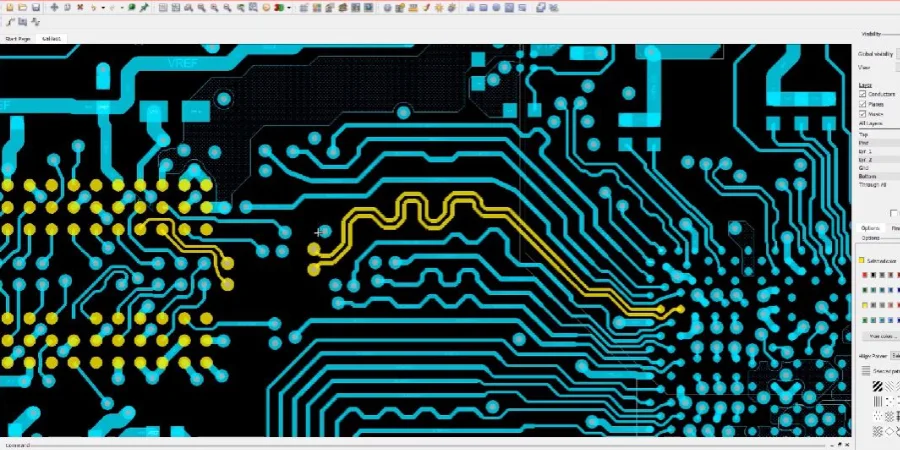
Routing high frequency signals demands precision that low-frequency designs never require. At frequencies above 100 MHz, every trace becomes a transmission line where geometry, spacing, and transitions directly impact signal quality. Poor routing choices create impedance discontinuities, excessive loss, and crosstalk that can render a design non-functional.
This guide provides practical routing strategies for high frequency PCB design, covering the principles and techniques that separate successful HF designs from failed ones.
HILPCB specializes in high frequency PCB manufacturing with controlled impedance (±5% standard, ±3% critical), low-loss materials, and precision trace geometry for demanding RF and high-speed digital applications.
Why High Frequency Routing Differs From Standard Design
Standard PCB routing treats traces as simple wires connecting two points. At high frequencies, this simplification fails completely. Signals propagating at gigahertz frequencies experience the trace as a distributed electromagnetic structure where every geometric feature affects performance.
At HILPCB, our engineering team applies transmission line principles to every high frequency design, ensuring signal integrity from driver to receiver across the complete frequency range.
Core Differences in HF Routing
- Transmission Line Behavior: When trace length exceeds 1/10 of signal rise time distance, traces become transmission lines requiring impedance control. A 1ns rise time signal in FR-4 transitions to transmission line behavior at approximately 0.6 inches.
- Wavelength Considerations: At 1 GHz in FR-4, signal wavelength is approximately 150mm. At 10 GHz, this shrinks to 15mm. Even short traces exhibit distributed behavior at high frequencies.
- Impedance Sensitivity: A 10% impedance variation creates measurable reflections. A 30% discontinuity causes significant signal degradation with ringing and timing errors.
- Loss Mechanisms: Skin effect, dielectric absorption, and surface roughness losses all increase with frequency, making material selection and geometry optimization critical.
- Coupling Effects: Crosstalk that is negligible at 100 MHz becomes destructive at 5 GHz. Spacing rules become mandatory rather than optional.
- Return Path Requirements: High frequency return current flows directly beneath the signal trace. Any interruption in this path creates inductance that distorts signals.
Design Philosophy Shift
HF routing is not about connecting points with minimum wire length—it's about creating controlled-impedance transmission lines with minimal discontinuities, appropriate loss characteristics, and adequate isolation. Every routing decision impacts signal quality: trace width affects impedance, spacing affects crosstalk, length affects delay and loss, and transitions affect reflections.
Understanding these fundamental differences enables designers to make informed tradeoffs between routing density, signal performance, and manufacturing cost. The subsequent sections address each critical aspect of HF routing methodology.
Transmission Line Structures and Impedance Control
Characteristic impedance is the fundamental parameter governing high frequency signal propagation. Maintaining consistent impedance throughout the signal path prevents reflections that degrade signal quality.
HILPCB provides comprehensive impedance control services with ±5% tolerance for standard applications and ±3% for critical RF designs, verified through 100% TDR testing on production panels.
Microstrip Configuration
Microstrip places signal traces on outer layers with a reference plane below. The electromagnetic field extends partially into air (Dk=1) and partially into the substrate, creating an effective dielectric constant lower than the bulk material. Microstrip impedance depends on trace width (W), substrate height (H), dielectric constant (Dk), and copper thickness (T).
- Typical impedance range: 30Ω to 120Ω achievable
- Advantages: Component access, easier routing, lower propagation delay
- Limitations: Field radiation above ~10 GHz, less predictable Dk variation
- Best applications: Moderate frequency (<5 GHz), short traces, component-dense areas
Stripline Configuration
Stripline buries traces between two reference planes, creating symmetric field distribution entirely within the dielectric. This eliminates radiation and provides superior shielding but requires via transitions to reach components.
- Typical impedance range: 35Ω to 90Ω practical range
- Advantages: No radiation, better shielding, predictable Dk, lower crosstalk
- Limitations: Via transitions required, slightly higher loss
- Best applications: Critical high frequency signals, long runs, crosstalk-sensitive designs
Common Impedance Targets
| Interface | Single-Ended | Differential |
|---|---|---|
| RF/Coax | 50Ω | — |
| Video | 75Ω | — |
| USB 3.x | — | 90Ω |
| PCIe | — | 85Ω |
| DDR4/5 | — | 80-90Ω |
| HDMI | — | 100Ω |
Achieving Target Impedance
Calculate trace width using field solvers or impedance calculators specific to your stackup. Never copy trace widths from other designs—different materials and layer spacing require different geometries for the same impedance. Specify impedance requirements to your manufacturer rather than geometry; the fabricator adjusts trace width based on actual material Dk and process parameters.
Layer Stack Strategy for High Frequency Signals
Layer assignment profoundly affects high frequency signal quality. Strategic stackup design provides the foundation for successful routing before a single trace is placed.
HILPCB High Frequency Stackup Capabilities
At HILPCB, our stackup engineering team optimizes layer arrangements for signal integrity, manufacturability, and cost-effectiveness across applications from consumer electronics to aerospace systems.
Signal-to-Plane Coupling
Every high frequency signal layer must be adjacent to a continuous reference plane. At high frequencies, return current flows directly beneath the signal trace through displacement current in the dielectric. Placing signals next to planes with gaps, splits, or discontinuities forces return current to detour, creating loop inductance that causes ringing and EMI.
- Route high-speed signals only on layers with solid adjacent planes
- Avoid crossing plane splits with any high frequency trace
- Use ground planes for reference when possible (more stable than power planes)
Layer Pairing Strategy
For multi-layer boards, pair signal layers with their reference planes consistently. The 4-layer configuration uses Signal-Ground-Power-Signal with HF signals on layers 1 and 4. The 6-layer uses Signal-Ground-Signal-Signal-Power-Signal for HF on layers 1 and 3. The 8-layer configuration provides Signal-Ground-Signal-Ground-Power-Signal-Power-Signal for maximum flexibility.
Material Considerations
Different layers may use different materials in hybrid stackups. Place high frequency signals on layers using low-loss materials (Rogers, Taconic, low-Df FR-4) while using standard FR-4 for power distribution and low-speed signals. This optimizes cost while maintaining HF performance. HILPCB offers hybrid lamination services combining materials to reduce cost by 40-60% versus all-HF-material stackups.
Routing Methodology for Critical High Frequency Nets
Systematic routing methodology ensures consistent results across complex high frequency designs. Following a structured approach prevents errors that are difficult to diagnose after layout completion.
At HILPCB, our DFM review process validates routing methodology for high frequency designs, identifying potential signal integrity issues before manufacturing.
Pre-Routing Planning
Before placing any traces, complete these preparatory steps:
- Classify all nets by frequency and criticality (critical HF, moderate HF, low frequency)
- Define impedance requirements for each net class
- Establish spacing rules based on crosstalk budget
- Identify layer assignments for each signal class
- Plan via strategies for layer transitions
- Review component placement for routing efficiency
Routing Priority Sequence
Route signals in order of decreasing sensitivity. Start with highest frequency analog/RF traces that are most sensitive to discontinuities and coupling. Follow with high-speed differential pairs for SerDes, USB, and PCIe requiring matched pairs. Route clock signals next as they are timing-critical and potential aggressors. Then complete high-speed single-ended signals, power distribution, low-speed digital, and finally ground connections.
Routing Best Practices
- Minimize length: Every inch adds loss and delay. Place components to minimize HF trace lengths.
- Maintain consistency: Keep trace width constant. Avoid necking down except at pad entries.
- Avoid stubs: Open-ended trace segments create reflections. Route point-to-point without branches.
- Reference plane continuity: Never cross plane gaps. Add stitching vias if plane transition is unavoidable.
- Controlled layer transitions: Minimize vias on critical signals. When required, use optimized via structures.
- Length matching: Match differential pair lengths within ±5 mils for multi-Gbps signals.
Documentation Requirements
Document all routing constraints in design rules and fabrication notes. Include impedance targets, spacing requirements, and any special manufacturing instructions. Clear documentation prevents manufacturing variations from degrading carefully designed signal integrity.
Via Design and Layer Transition Management
Vias represent significant discontinuities in high frequency signal paths. Each via introduces impedance change, stub resonance, and additional loss. Managing via impact is essential for successful HF routing.
HILPCB offers back-drilling services with residual stub less than 10 mils, blind/buried vias, and via-in-pad with filled and capped options for optimal high frequency performance.
Via Electrical Model
A via comprises several elements affecting high frequency behavior. The barrel inductance acts as an inductor, typically 0.5-1.5 nH depending on length and diameter. Pads on signal and reference layers add capacitance, typically 0.3-0.8 pF per pad. Unused barrel length below the exit layer creates a resonant stub. Clearance holes in planes affect return path and add capacitance.
Via Impedance Optimization
Via impedance differs from trace impedance, creating discontinuities. Smaller via diameter reduces inductance and capacitance—use 8-10 mil drill for HF signals versus 12-14 mil standard. Minimum annular ring reduces pad capacitance. Larger anti-pads reduce capacitance but may affect return path. Ground vias adjacent to signal vias provide return path continuity.
Stub Management
Via stubs create resonances that notch the frequency response. The first resonance occurs when stub length equals quarter wavelength. For a 60-mil stub in FR-4, resonance occurs at approximately 9 GHz, causing significant signal attenuation.
- Back-drilling: Remove unused barrel after plating. HILPCB achieves <10 mil residual stub.
- Blind/buried vias: Use vias spanning only required layers, eliminating stubs entirely.
- Via-in-pad: When vias must be in pads, use filled and capped vias to prevent solder wicking.
Frequency-Based Via Selection
Below 3 GHz, standard through-hole vias are acceptable. From 3-10 GHz, minimize via count and consider back-drilling. From 10-25 GHz, back-drilling is required with blind/buried preferred. Above 25 GHz, use blind/buried vias with extensive optimization for every transition.
Material Selection and Loss Management
Material properties fundamentally limit achievable performance in high frequency routing. Selecting appropriate materials for your frequency range and loss budget prevents designing circuits that cannot be manufactured successfully.
At HILPCB, we maintain extensive inventory of high frequency materials including Rogers, Taconic, Isola, and Panasonic laminates, with engineering support for material selection and hybrid stackup optimization.
Key Material Parameters
- Dielectric constant (Dk): Affects impedance and propagation delay. Lower Dk enables wider traces and faster propagation.
- Dissipation factor (Df): Determines dielectric loss. Lower Df means less signal attenuation.
- Dk stability: Variation with frequency affects wideband performance. Stable Dk simplifies design.
- Copper roughness: Surface roughness increases loss at high frequencies due to skin effect.
Material Selection by Frequency
Standard FR-4 with Df of 0.020-0.025 suits frequencies below 1 GHz. Mid-loss FR-4 variants like Isola FR408HR with Df of 0.008-0.015 work for 1-5 GHz. Low-loss materials like Rogers RO4350B with Df of 0.003-0.006 serve 5-15 GHz applications. Very low-loss options with Df of 0.001-0.003 handle 15-40 GHz. PTFE and ceramic materials with Df below 0.001 support frequencies above 40 GHz.
Hybrid Stackup Strategy
Use expensive low-loss materials only where needed. Place high frequency signals on low-loss laminate layers while using standard FR-4 for power distribution and low-speed signals. This reduces material cost by 40-60% while maintaining HF performance. HILPCB provides engineering support for hybrid stackup design and lamination.
Loss Budget Planning
Calculate total path loss at your operating frequency including conductor loss (increases with √f), dielectric loss (increases linearly with f), via losses (fixed per transition), and connector losses. Compare total loss against receiver sensitivity and equalization capability. If loss exceeds budget, reduce trace length, upgrade materials, or both.
Related High Frequency Routing Topics
- Trace Layout for High Frequency PCB: Detailed trace geometry and placement strategies
- Routing Clearance in HF PCB: Spacing rules for crosstalk control
- Corner Routing for High Frequency PCB: Bend and corner optimization techniques
- Trace Length Control in HF PCB: Length matching and delay management
- Routing Discontinuity in HF PCB: Managing impedance transitions
HILPCB High Frequency Routing Services
HILPCB delivers manufacturing precision that preserves your carefully designed signal integrity:
Design Support: Pre-manufacturing DFM review, stackup optimization, impedance modeling, and material recommendations for your specific frequency requirements.
Manufacturing Precision: Controlled impedance with ±5% standard and ±3% critical tolerance, precise trace geometry, and consistent dielectric thickness across production lots.
Advanced Processes: Back-drilling, blind/buried vias, via-in-pad, and hybrid material lamination for demanding high frequency applications.
Verification: 100% TDR testing on controlled impedance, VNA characterization available to 67 GHz, and comprehensive quality documentation.
From rapid prototypes through volume production, HILPCB provides consistent high frequency PCB quality with turnkey assembly including precision placement of RF components.
Contact HILPCB for high frequency PCB design review and manufacturing quotation.
Common Questions
Why is routing discipline so important in high-frequency PCB design?
Because at high frequency, interconnect geometry becomes part of the electrical system. Small routing mistakes can change impedance, increase loss, and degrade signal integrity enough to affect final product performance.
Which routing rules matter most on high-frequency boards?
Controlled impedance, short return paths, stable reference planes, minimized discontinuities, and consistent spacing are usually the core rules. Good stackup planning and material selection are just as important as the trace pattern itself.
Why do vias and connectors need special attention?
They often create the biggest discontinuities in an otherwise clean RF or high-speed channel. Via stubs, poor launches, and inconsistent transitions can introduce reflection and loss that dominate channel behavior.
How does manufacturing support help verify a routing design?
DFM review, impedance modeling, TDR results, and process control all help confirm that the manufactured board matches the design intent. Without that feedback loop, a theoretically correct layout may still underperform in production.