
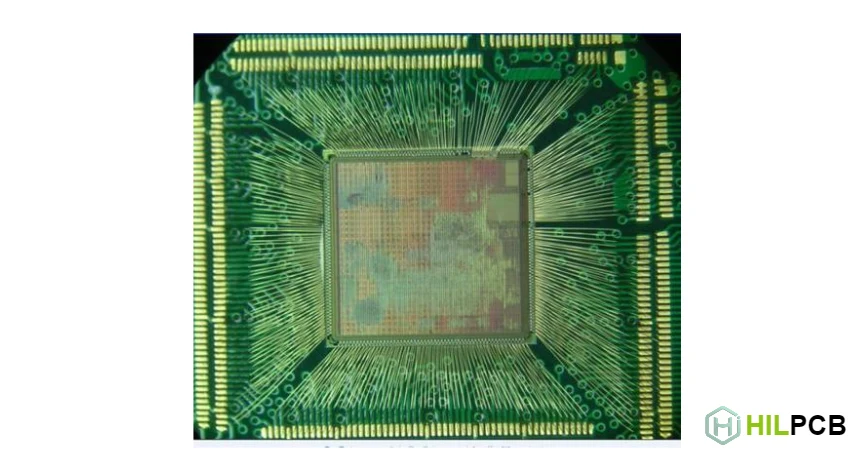
Fine pitch BGA packages with ball pitches of 0.5mm and below enable the high I/O density required for modern processors, memory devices, and system-on-chip solutions. These advanced packages demand manufacturing capabilities beyond standard BGA assembly, including tighter process tolerances, specialized PCB construction, and enhanced inspection methods.
HILPCB provides fine pitch BGA assembly services with the equipment precision, process control, and inspection capabilities these demanding packages require.
Menu Navigation
- Defining Fine Pitch BGA Packages
- PCB Requirements for Fine Pitch Assembly
- Stencil Design for Fine Pitch BGAs
- Placement Accuracy Requirements
- Reflow Considerations for Fine Pitch
- Inspection Challenges and Solutions
- HILPCB Fine Pitch Assembly Services
Defining Fine Pitch BGA Packages
Fine pitch designates BGA packages with ball spacing tighter than the 0.8mm threshold where standard assembly processes begin requiring significant modification. As pitch decreases, all aspects of the assembly process demand proportionally tighter control.
Understanding the relationship between pitch and process requirements helps designers make informed packaging decisions and enables manufacturers to allocate appropriate resources.
Pitch Categories and Characteristics
- Standard Pitch (0.8mm-1.27mm): Conventional BGA with comfortable process margins; standard stencils and placement equipment adequate; visual inspection of peripheral balls feasible.
- Fine Pitch (0.5mm-0.65mm): Requires enhanced placement accuracy and stencil optimization; HDI PCB typically necessary; X-ray inspection essential.
- Ultra-Fine Pitch (0.4mm): Demands precision equipment and tight process control; HDI mandatory; advanced inspection methods required.
- Micro Pitch (<0.4mm): Extreme precision requirements; specialized substrates and processes; advanced packaging expertise essential.
Package Types in Fine Pitch Category
- Chip Scale Packages (CSP): Package area near die size (≤1.2x); ball pitches 0.4mm-0.65mm typical; used extensively in mobile devices and wearables.
- Wafer Level Packages (WLP/WLCSP): Die with redistributed pads; pitches as low as 0.3mm; requires HDI substrate with microvias.
- Flip Chip BGA (FCBGA): High-performance processors with fine pitch peripheral area; interior array may be coarser pitch; complex routing requirements.
- Package-on-Package (PoP): Stacked configurations with fine pitch interfaces; memory-on-logic common in smartphones; requires precise stacking alignment.
- Fan-Out Wafer Level (FOWLP): Emerging technology with reconstituted wafer approach; I/O redistributed to larger area; pitch depends on redistribution design.
Application Drivers
Fine pitch packages dominate in applications requiring high functionality in constrained space, driving adoption across consumer electronics, computing, and communications.
PCB Requirements for Fine Pitch Assembly
Fine pitch BGAs impose stringent requirements on PCB construction that standard fabrication processes cannot meet. HDI (High Density Interconnect) technology provides the routing density and feature precision these packages demand.
PCB capability limits practical pitch for any given design. Manufacturing partnership between PCB fabrication and assembly ensures compatible capability across the production chain.
HDI PCB Technologies
- Microvia Construction: Laser-drilled vias with diameters 0.1mm or smaller; single-layer connections (1+N+1) or sequential lamination for higher density.
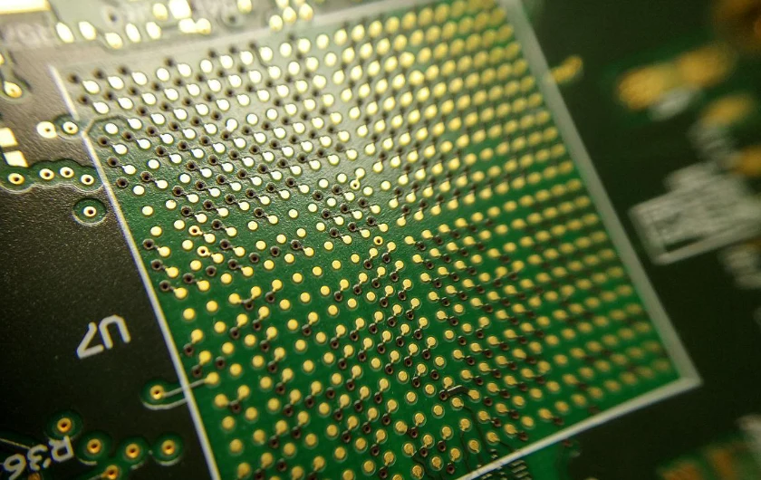
- Via-in-Pad: Microvias directly under BGA pads enable routing density; filled and capped construction prevents solder wicking and voiding.
- Build-Up Layers: Sequential lamination adds routing layers outside the core; typical configurations 2+4+2 or higher for dense designs.
- Fine Line Capability: Trace widths and spaces of 75μm or finer enable escape routing; 50μm capabilities for most aggressive designs.
- Registration Accuracy: Layer-to-layer alignment within ±50μm or better ensures via and pad alignment; tighter registration reduces yield but improves design margin.
Pad Design Requirements
- NSMD Preference: Non-solder mask defined pads provide superior joint strength and inspection visibility; solder mask registration critical for fine pitch.
- Pad Size Optimization: Smaller pads for fine pitch balance joint strength with bridging prevention; typical 80-85% of ball diameter for NSMD.
- Solder Mask Registration: Fine pitch demands tight solder mask-to-copper registration; ±25μm required for 0.4mm pitch; advanced imaging technologies.
- Surface Finish Flatness: ENIG preferred for consistent, flat surface; immersion finishes must meet planarity requirements for fine pitch.
Routing and Escape Strategies
Signal escape from dense fine pitch arrays requires sophisticated routing strategies exploiting HDI capability.
- Dog-Bone Escape: Traditional pattern with via offset from pad; limited by minimum trace and via spacing.
- Via-in-Pad Escape: Direct via placement enables single-layer escape for many signals; requires filled and planarized vias.
- Multi-Layer Escape: Complex arrays require signals routed on multiple layers; sequential escape reduces layer count requirements.
- Controlled Impedance: High-speed signals demand impedance-controlled routing; trace geometry must accommodate both escape density and electrical requirements.
Stencil Design for Fine Pitch BGAs
Solder paste stencil design critically affects fine pitch BGA assembly success. Reduced aperture sizes challenge paste transfer efficiency while demanding precise volume control to prevent both opens and bridges.
Stencil technology selection and aperture engineering optimize paste deposition for fine pitch requirements.
Stencil Technology Options
- Laser-Cut Stainless Steel: Standard technology with aperture walls showing cut marks; adequate for 0.5mm pitch; wall quality affects paste release.
- Electroformed Nickel: Smooth, tapered aperture walls provide superior paste release; preferred for 0.4mm and finer pitch; higher cost justified by yield improvement.
- Laser-Cut with Electropolishing: Post-cut smoothing improves wall finish; intermediate option between laser-cut and electroformed.
- Nano-Coated Stencils: Surface treatments reduce paste adhesion to aperture walls; improves transfer efficiency particularly for fine apertures.
Aperture Design Principles
- Area Ratio Rule: Aperture area divided by wall area determines paste release; ratio >0.66 required for reliable transfer; finer pitch requires reduced stencil thickness.
- Thickness Selection: Finer pitch requires thinner stencils to maintain area ratio; 0.4mm pitch typically uses 80-100μm thickness; step-down for fine pitch areas.
- Aperture Reduction: Apertures typically sized smaller than pads for fine pitch; prevents bridging while maintaining adequate volume; balances opens and shorts risk.
- Shape Optimization: Circular apertures release better than square; rounded corners reduce bridging; home plate shapes used in some applications.
Area Ratio Calculations
For reliable paste transfer, area ratio must exceed critical threshold based on paste characteristics and aperture geometry.
Area Ratio = Aperture Area / Wall Area
For circular apertures:
- Aperture Area = π × (d/2)²
- Wall Area = π × d × t
- Area Ratio = d / (4 × t)
Where d = aperture diameter, t = stencil thickness
For 0.4mm pitch with 0.35mm apertures and 100μm stencil:
- Area Ratio = 0.35 / (4 × 0.1) = 0.875 (acceptable)
For same apertures with 150μm stencil:
- Area Ratio = 0.35 / (4 × 0.15) = 0.58 (problematic)
Step Stencil Applications
Mixed assemblies with both fine pitch and large-pitch components may benefit from step stencils providing different paste volumes in different board areas.
- Step-Down Areas: Reduced thickness in fine pitch component areas provides appropriate area ratio.
- Step-Up Areas: Increased thickness for large components, connectors, or shields requiring more solder volume.
- Design Considerations: Step transitions require clearance from apertures; step locations planned during stencil design.
Placement Accuracy Requirements
Fine pitch BGA assembly demands placement accuracy proportionally tighter than standard pitch. Self-alignment during reflow assists positioning, but excessive initial error prevents proper joint formation.
Equipment capability and process control ensure consistent placement meeting fine pitch requirements.
Accuracy Specifications
- 3-Sigma Accuracy: Equipment specified for maximum deviation at statistical limits; fine pitch requires ±30-50μm at 3σ depending on pitch.
- Capability Index (Cpk): Statistical measure of process capability relative to specification; Cpk >1.33 ensures consistent accuracy.
- Angular Accuracy: Rotation error affects corner ball alignment more than center; tight angular tolerance essential for large fine pitch BGAs.
- Placement Force: Excessive force damages solder balls; fine pitch balls smaller and more vulnerable; force control systems prevent damage.
Machine Requirements
- Vision System Resolution: Camera resolution and optics must resolve fine pitch features; fiducial recognition accuracy affects placement accuracy.
- Pattern Recognition: Ball pattern recognition for fine pitch requires advanced algorithms; component inspection before placement identifies damaged devices.
- Motion System Precision: Linear motors and encoders provide positioning repeatability; thermal stability maintains calibration over production shifts.
- Calibration Maintenance: Regular verification ensures continued accuracy; drift monitoring between calibration cycles.
Process Factors Affecting Placement
- Paste Condition: Fresh, properly conditioned paste supports component weight; slumped or degraded paste allows drift before reflow.
- Placement Sequence: Lighter components after heavy to prevent disturbance; BGA placement timing minimizes paste exposure.
- Transfer Efficiency: Component transport from feeder to board without shift or rotation; vacuum levels and nozzle condition affect consistency.
- Environmental Factors: Temperature and humidity affect paste behavior; controlled environment maintains process stability.
Reflow Considerations for Fine Pitch
Fine pitch BGAs present specific reflow challenges including reduced thermal mass of smaller solder balls and tighter tolerances for temperature uniformity across the joint array. Profile optimization balances these factors while maintaining soldering defect prevention.
The smaller solder volume in fine pitch joints provides less thermal capacity, affecting both heating behavior and solidification.
Thermal Profile Considerations
- Heating Uniformity: Temperature variation across fine pitch array must remain minimal; gradients cause differential melting timing and warpage-related defects.
- Time Above Liquidus: Shorter TAL appropriate for fine pitch due to smaller thermal mass; excessive TAL promotes intermetallic growth in thin joints.
- Peak Temperature: Adequate peak ensures complete wetting; excessive peak increases warpage and may damage temperature-sensitive devices.
- Cooling Rate: Controlled cooling develops proper grain structure; fine pitch joints cool faster than large-pitch, potentially requiring profile adjustment.
Warpage Sensitivity
Fine pitch packages often exhibit greater warpage effects due to larger die-to-package size ratio and thinner construction.
- Dynamic Warpage: Warpage changes throughout thermal profile; maximum warpage may occur at temperature transitions.
- Package Specifications: Critical packages require warpage data from suppliers; assembly qualification includes warpage assessment.
- Mitigation Strategies: Reflow atmosphere, profile optimization, and board support reduce warpage-related defects.
Atmosphere Control
- Nitrogen Benefit: Inert atmosphere reduces oxidation during reflow; particularly beneficial for fine pitch where flux quantity is limited and joint volume small.
- Oxygen Level: Target <500ppm oxygen for fine pitch applications; lower levels for most challenging packages.
- Cost Consideration: Nitrogen consumption adds process cost; benefit versus cost evaluated for specific applications.
Inspection Challenges and Solutions
Fine pitch BGA inspection compounds standard BGA inspection challenges with reduced feature size and tighter defect tolerances. Inspection methods and equipment must match the demanding requirements.
Comprehensive inspection strategy combines multiple techniques to ensure thorough defect detection.
X-Ray Inspection Requirements
BGA X-ray inspection becomes even more critical for fine pitch packages where defect types are the same but feature sizes smaller.
- Resolution Requirements: Imaging resolution must distinguish individual balls; pixel size significantly smaller than ball diameter required.
- Magnification Capability: Higher magnification needed to visualize fine pitch details; geometric magnification with microfocus sources.
- Void Measurement: Smaller balls make void percentage assessment more challenging; higher resolution enables accurate measurement.
- 3D Imaging Value: Computed tomography particularly valuable for fine pitch; overlapping features in 2D images resolved in 3D reconstruction.
Automated Optical Inspection
AOI capabilities for fine pitch require enhanced resolution and specialized algorithms.
- Camera Resolution: Higher pixel density required for fine pitch feature detection; multi-resolution systems accommodate varied component sizes.
- Solder Paste Inspection: 3D SPI critical for fine pitch; volume measurement at small apertures requires precision sensors.
- Post-Reflow Limitations: Peripheral ball visibility limited even with enhanced resolution; X-ray remains primary BGA inspection method.
Electrical Test Considerations
- Boundary Scan: IEEE 1149 test access provides BGA connectivity verification without physical probing; essential for fine pitch where probe access impossible.
- Functional Test: Exercises device operation confirming connectivity and function; complements visual and X-ray inspection.
- Coverage Analysis: Test coverage analysis identifies connections not verified by available methods; design modification may improve testability.
HILPCB Fine Pitch Assembly Services
HILPCB provides fine pitch BGA assembly capabilities supporting packages from standard 0.5mm pitch through challenging 0.4mm and finer applications. Our investment in precision equipment, process development, and inspection technology enables reliable production of demanding designs.
Why Choose HILPCB for Fine Pitch BGA
Precision Placement Equipment
Our placement machines deliver the accuracy fine pitch packages demand. Placement capability down to 0.3mm pitch with accuracy specifications meeting IPC Class 3 requirements ensures consistent first-pass yield.
Advanced Stencil Technology
Fine pitch applications benefit from appropriate stencil selection:
- Electroformed stencils for ultra-fine pitch
- Nano-coated options for improved paste release
- Step stencil capability for mixed assemblies
HDI PCB Capability
Our HDI PCB fabrication supports fine pitch routing requirements:
- Microvia technology for via-in-pad designs
- Fine line capability for dense escape routing
- Tight registration for solder mask alignment
Optimized Reflow Processing
Nitrogen atmosphere reflow with precise profile control addresses fine pitch thermal requirements. Profiling capability ensures optimal results for specific package and board combinations.
Comprehensive Inspection
- High-resolution solder paste inspection verifies stencil printing
- X-ray inspection with resolution for fine pitch defect detection
- 3D capability for challenging defect types
Rework Capability
When defects occur, our BGA rework stations support fine pitch repair with the precision alignment these packages require. Reballing services restore components when ball restoration is needed.
Production Flexibility
- Prototype assembly for design validation with full inspection
- Small batch production with fine pitch process optimization
- Volume production with statistical process control
Contact HILPCB for fine pitch BGA assembly services. Our engineering team reviews your design requirements and provides specific recommendations for successful production.