
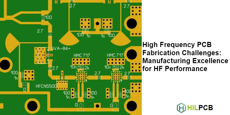
High frequency PCB fabrication demands manufacturing precision that standard processes cannot deliver. At microwave frequencies, variations that are invisible at lower frequencies—trace width deviations, copper surface texture, dielectric thickness inconsistency—directly impact impedance, loss, and signal integrity. Successful HF fabrication requires understanding these challenges and implementing processes that control variation within the tight tolerances high frequency performance demands.
This guide provides comprehensive knowledge of HF PCB fabrication challenges, from fundamental manufacturing physics through practical solutions that deliver consistent high frequency performance across production volumes.
HILPCB specializes in high frequency circuit board manufacturing with precision process control, advanced materials handling, and engineering expertise for overcoming the fabrication challenges unique to RF and microwave applications.
For release decisions, pair this fabrication overview with the high-frequency PCB owner page and the PCB quality evidence guide so inspection methods and records match the actual RF risk.
In this article:
- Why HF PCB Fabrication Differs From Standard Manufacturing
- Critical Process Parameters for HF Fabrication
- Material-Specific Manufacturing Challenges
- Process Control for Consistent Results
- Verification and Testing
- Design Guidelines for Manufacturability
Why HF PCB Fabrication Differs From Standard Manufacturing
Standard PCB manufacturing tolerances adequate for digital and low-frequency analog circuits become unacceptable at high frequencies. The same manufacturing variation that causes negligible impact at 100 MHz can render a 10 GHz circuit non-functional.
At HILPCB, our precision PCB manufacturing processes are specifically optimized for high frequency requirements that standard processes cannot meet.
Impedance Sensitivity
High frequency circuits require controlled impedance, typically within ±5% or tighter. Impedance depends on trace width, dielectric thickness, and material properties—all subject to manufacturing variation. A 10% trace width variation creates approximately 5% impedance change. Combined with dielectric variations, standard processes can easily exceed impedance tolerances.
At 10 GHz, even small impedance discontinuities cause measurable reflections. The manufacturing precision required increases with frequency as wavelengths shrink and discontinuities become electrically larger relative to signal wavelength.
Loss Sensitivity
Signal attenuation at high frequencies depends on conductor surface roughness and dielectric properties. Standard copper roughness that's irrelevant at 1 GHz adds significant loss at 10 GHz and above. Dielectric loss increases linearly with frequency, making material consistency critical. Manufacturing processes must preserve the low-loss properties of expensive HF materials.
Dimensional Criticality
At microwave frequencies, physical dimensions directly correspond to electrical behavior. A quarter-wave stub at 10 GHz is only about 4mm long in FR-4—manufacturing variation of 0.1mm represents 2.5% length error. Distributed elements, filters, and matching networks require dimensional accuracy that challenges standard fabrication processes.
Material Handling Challenges
High frequency materials often differ significantly from FR-4 in processing behavior. PTFE-based materials require surface treatment for adhesion. Ceramic-filled materials may have different drilling and routing characteristics. Hybrid stackups combining different materials create lamination challenges. These material differences demand specialized processing knowledge, particularly for PTFE circuit board fabrication.
Critical Process Parameters for HF Fabrication
Several manufacturing parameters particularly affect high frequency performance. Understanding and controlling these parameters enables consistent HF results.
Trace Width Control
Trace width directly affects impedance. For controlled impedance, width tolerance typically needs to be ±10% or better. Achieving this requires controlled imaging (exposure consistency, develop uniformity), controlled etching (etch rate uniformity, compensation accuracy), and thick copper management (etch factor increases with copper weight).
For fine lines below 4 mils, advanced imaging and etching processes become necessary. HILPCB maintains etching precision for HF PCB through statistical process control and optimized chemistry.
Dielectric Thickness
Dielectric thickness between signal and reference plane affects impedance proportionally. Standard tolerance of ±10% may be adequate for some applications, but critical circuits may require ±5% or better. Dielectric thickness control depends on prepreg flow during lamination, core thickness consistency, and copper pattern density effects on prepreg thickness.
Copper Thickness
Copper weight affects impedance slightly but significantly impacts current capacity and loss. Plating uniformity ensures consistent copper across the panel. The effects of copper thickness on impedance must be included in design calculations. Understanding copper roughness effects in HF PCB manufacturing is essential for loss control.
Registration
Layer-to-layer alignment affects differential pair balance, via-to-pad alignment, and stripline symmetry. High frequency circuits may require tighter registration than standard processes provide. Automated optical inspection verifies registration meets requirements, as detailed in registration tolerance for HF PCB manufacturing.
HILPCB HF Manufacturing Capabilities
Material-Specific Manufacturing Challenges
Different high frequency materials present unique fabrication challenges. Successful manufacturing requires material-specific process knowledge.
PTFE and Fluoropolymer Materials
PTFE (Teflon) provides excellent electrical properties but presents significant manufacturing challenges. The non-stick surface that makes PTFE useful electrically also resists adhesion to copper and other materials. Surface treatment (plasma, chemical, or mechanical) is required before lamination.
PTFE materials are soft and can smear during drilling, requiring optimized drill parameters. They also have high CTE, requiring careful thermal management during processing. HILPCB maintains specialized processes for fluoropolymer PCB manufacturing that address these challenges.
Ceramic-Filled Materials
Ceramic fillers improve electrical properties but create mechanical processing challenges. The hard ceramic particles wear drill bits faster. Routing and scoring require appropriate tooling. Laser processing may behave differently than with unfilled materials.
Hybrid Stackups
Combining different materials in one stackup—common for cost optimization—creates lamination challenges. Different materials have different lamination temperatures and pressures. CTE mismatch can cause warpage or stress. Bonding between different materials requires appropriate prepreg selection. The process expertise for hybrid stackups is detailed in lamination accuracy for high frequency PCB manufacturing.
Low-Loss FR-4 Variants
Enhanced FR-4 materials offer better HF performance with more familiar processing. However, some low-loss variants have different resin systems that may require adjusted processing parameters. Material-specific data sheets should guide process parameters.
Process Control for Consistent Results
Achieving consistent high frequency performance requires rigorous process control that goes beyond standard manufacturing practices.
Statistical Process Control
SPC monitors critical parameters continuously, identifying drift before it causes defects. Control charts track trace width, dielectric thickness, impedance, and other critical parameters. Process capability indices (Cpk) quantify ability to meet specifications. Regular capability studies verify processes remain in control.
In-Process Measurement
Measure critical parameters during fabrication, not just at final inspection. Impedance test coupons measured during build enable process adjustment. Cross-section analysis verifies internal dimensions. Automated optical inspection catches defects early.
Material Lot Control
High frequency materials can vary between lots. Incoming inspection verifies material properties. Lot traceability enables correlation of performance with material source. Qualified material sources reduce variation risk.
Environmental Control
Temperature and humidity affect manufacturing processes. Controlled environment in critical process areas ensures consistent results. Material storage conditions prevent moisture absorption and property changes. These factors contribute to overall yield control for HF PCB manufacturing success.
Verification and Testing
Comprehensive testing verifies that fabrication meets high frequency requirements.
Impedance Testing
TDR (Time Domain Reflectometry) testing measures characteristic impedance along trace length. 100% testing of controlled impedance traces is standard for HF boards. Coupons and actual circuit traces both provide useful data. HILPCB performs comprehensive impedance verification on all controlled impedance boards.
Dimensional Verification
Automated optical inspection measures trace widths and spacing. Cross-sectioning verifies internal dimensions and layer alignment. These measurements verify process control effectiveness and support continuous improvement.
Electrical Testing
Continuity and isolation testing verify basic functionality. High-frequency characterization (S-parameters, insertion loss) may be required for critical applications. VNA testing to 67 GHz available for demanding applications at HILPCB.
Material Verification
Verify material properties match specifications. Incoming inspection and test coupons provide data. Dk and Df verification ensures electrical performance will meet requirements.
Design Guidelines for Manufacturability
Design choices significantly impact manufacturing success. Following guidelines improves yield and performance.
Tolerance Allocation
Allocate tolerance budget across manufacturing variables. Don't specify tighter tolerance than necessary. Understand which parameters most affect your circuit performance. Communicate critical requirements clearly in fabrication notes.
Feature Size Selection
Larger features are easier to manufacture accurately. Use minimum feature sizes only where necessary. Consider copper weight effects on achievable feature sizes. Wider traces have lower percentage variation for same absolute tolerance.
Material Selection
Select materials appropriate for manufacturing capability. Exotic materials require specialized processing. Consider hybrid stackups to optimize cost and performance. Discuss material options with your fabricator early in design.
Documentation
Clear documentation prevents manufacturing errors. Specify impedance requirements, not just geometry. Identify critical features requiring particular attention. Include stackup details with material specifications. HILPCB provides DFM review to identify potential issues before manufacturing.
For demanding applications, HILPCB offers comprehensive Rogers laminate fabrication with full engineering support.
HILPCB HF Fabrication Services
HILPCB delivers manufacturing excellence for high frequency PCB challenges:
Process Precision: Statistical process control, optimized chemistry, and advanced imaging for trace geometry accuracy.
Material Expertise: Specialized processing for PTFE, ceramic-filled, and hybrid stackups with material-specific optimization.
Advanced Testing: 100% TDR testing, VNA characterization to 67 GHz, and comprehensive dimensional verification.
Engineering Support: DFM review, stackup optimization, and manufacturing consultation for HF applications.
From RF prototype development through volume HF production, HILPCB provides comprehensive HF manufacturing capabilities with turnkey assembly services.
Contact HILPCB for HF fabrication consultation and manufacturing quotation.
Common Questions
Why is high frequency PCB fabrication harder than standard PCB manufacturing?
Small variations in trace geometry, dielectric thickness, and copper surface condition can change impedance and loss at RF and microwave frequencies.
Which fabrication parameters matter most for HF performance?
Etching precision, copper roughness, dielectric thickness control, and registration accuracy are usually the most critical manufacturing variables.
How does process control improve HF yield?
Tight process control reduces unit-to-unit variation and helps more boards meet insertion loss, impedance, and return loss targets on the first pass.
What tolerances are typical in RF and microwave PCB work?
Exact values depend on frequency and stackup, but HF jobs usually require tighter impedance, thickness, and alignment limits than general-purpose boards.