
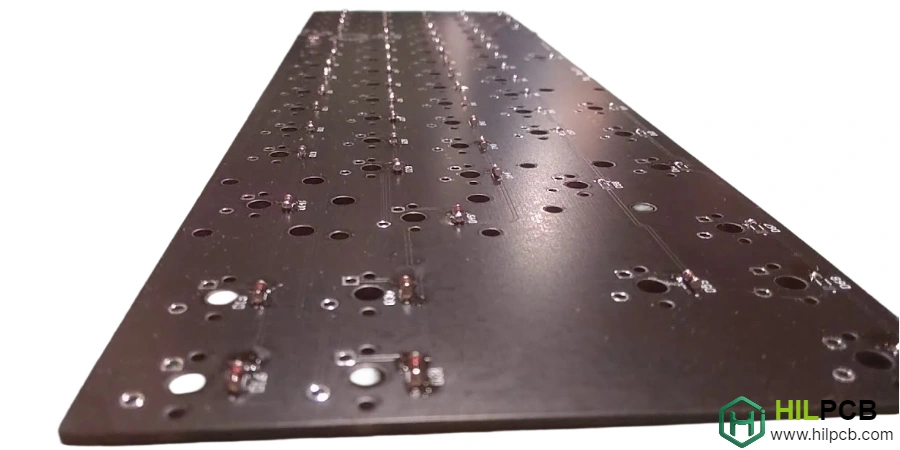
The quality of a mechanical keyboard ultimately depends on the precision and consistency of its PCB manufacturing. From circuit board fabrication to component assembly, every step in the Mechanical Keyboard PCB Manufacturing process affects the final product's performance, reliability, and user experience. Understanding this process helps keyboard designers and brands make informed decisions about production partners and quality requirements.
This comprehensive guide explores the complete manufacturing workflow for keyboard PCBs, highlighting critical processes, quality control measures, and best practices that separate exceptional products from mediocre ones.
Menu Navigation
- PCB Fabrication Process for Keyboards
- Component Assembly and SMT Processing
- Quality Control and Testing Protocols
- Production Scaling: Prototype to Volume
- Optimizing Cost Without Compromising Quality
PCB Fabrication Process for Keyboards
PCB fabrication transforms design files into physical circuit boards through a series of precise manufacturing steps. Each stage requires careful control to produce boards that meet keyboard-specific requirements for switch mounting, durability, and electrical performance.
1. Material Preparation and Layer Formation
The fabrication process begins with selecting appropriate base materials based on application requirements. Standard FR4 PCB serves most keyboard applications effectively. High-Tg FR4 provides better thermal stability for hot-swap boards with high-power RGB lighting. Flexible materials enable split keyboard connections and compact designs requiring bend capability.
Copper cladding weight selection directly impacts durability. 1oz copper (35μm) suits standard soldered keyboards. 2oz copper (70μm) is recommended for hot-swap configurations requiring enhanced pad strength. 2oz+ copper (70μm+) serves high-current applications with extensive LED arrays.
2. Circuit Pattern Transfer
Creating precise circuit patterns requires multiple carefully controlled steps. The imaging process converts design data to photographic film or direct laser imaging. Photoresist application to the copper surface enables pattern transfer. UV exposure through circuit patterns and subsequent development reveals copper for etching. Chemical etching removes unwanted copper with critical trace width accuracy—line width/space tolerance typically ±0.05mm for keyboard applications.
3. Drilling and Via Formation
Keyboard PCBs require numerous holes for switches, LEDs, and components. Mechanical drilling creates switch holes (3.0mm and 1.5mm for MX-style), stabilizer holes (various sizes for different mount types), and via holes (0.3-0.5mm typical). Through-hole vias serve standard 2-layer boards. Blind/buried vias enable Multi-Layer PCB for Keyboards. Microvias support HDI PCB applications requiring high-density routing.
4. Surface Finish Application
Surface finish protects exposed copper and ensures solderability throughout the product lifecycle. ENIG provides flat surfaces and long shelf life—ideal for hot-swap sockets and premium boards. HASL offers cost-effective proven reliability for budget keyboards. OSP enables lead-free assembly with flat surface characteristics. Hard Gold delivers extreme durability for edge connectors and high-wear applications.
Our Mechanical Keyboard PCB production supports all standard surface finishes with ENIG as the recommended option for hot-swap designs.

Component Assembly and SMT Processing
After bare PCB fabrication, Surface Mount Technology (SMT) assembly adds the components that bring the keyboard to life. This process requires precision equipment and controlled environments to ensure reliable solder joints and proper component function.
Solder Paste Application
The assembly process begins with precise solder paste deposition using laser-cut stainless steel stencils. Aperture design optimization for each component type ensures proper paste volume. Typical paste thickness ranges from 0.1-0.15mm for keyboard components. Solder Paste Inspection (SPI) systems verify paste volume accuracy, position alignment, and bridge detection before component placement.
Component Placement
High-speed pick-and-place machines position components with remarkable precision. Standard components achieve ±0.05mm accuracy while fine-pitch ICs require ±0.025mm precision. LED positioning demands particular attention for even lighting appearance across the keyboard.
Keyboard PCBs typically include microcontrollers (QFP, QFN packages), USB-C connectors (complex multi-pad footprints), ESD protection ICs, crystal oscillators, LED drivers and individual LEDs, and hot-swap sockets when pre-installed at the factory.
Reflow Soldering
Controlled heating creates reliable solder joints through a precise thermal profile. The preheat zone provides gradual temperature increase. The soak zone activates flux for proper wetting. The reflow zone melts solder at approximately 245°C peak for lead-free assembly. The cooling zone ensures controlled cool-down preventing thermal shock.
Critical considerations include USB-C connector heat sensitivity, LED thermal limits, and large ground plane heat sinking effects that require profile adjustment.
Our SMT Assembly lines maintain precise thermal profiles for consistent keyboard PCB results across production runs.
Quality Control and Testing Protocols
Mechanical Keyboard PCB Manufacturing requires rigorous quality control at multiple stages. Comprehensive testing ensures every board meets performance and reliability standards before reaching customers.
In-Process Inspection
Automated Optical Inspection (AOI) provides post-reflow inspection of all solder joints, component presence and polarity verification, solder bridge and insufficient solder detection, with 100% coverage of production units. X-ray inspection enables BGA and QFN package solder joint verification, hidden joint quality assessment, and sample or critical component inspection as required.
Electrical Testing
Bare board testing verifies continuity for all circuits, isolation between traces, and impedance characteristics for USB signal paths. Functional testing for assembled keyboard PCBs confirms USB enumeration and communication, key matrix scanning across all switch positions, LED driver functionality and lighting uniformity, and firmware boot and response characteristics.
Reliability Testing
Production samples undergo additional validation testing:
- Thermal Cycling: -40°C to +85°C across 100 cycles validates solder joint reliability.
- Humidity Exposure: 85% RH at 85°C for 168 hours confirms moisture resistance.
- Vibration Testing: Random vibration per IPC standards ensures mechanical durability.
- Hot-Swap Specific: Socket insertion/removal cycling (1000+ cycles), pad adhesion testing, and contact resistance measurement over time.
Quality Documentation
Comprehensive documentation ensures traceability through lot tracking for all materials, test data records, non-conformance reporting, and Certificate of Conformance (CoC) for shipments.
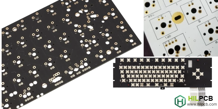
Production Scaling: Prototype to Volume
Successful keyboard projects require manufacturing partners who can scale smoothly from initial prototypes to volume production without compromising quality. Each production phase has distinct objectives and approaches.
Prototype Phase (1-50 Units)
The prototype phase focuses on design verification, functional testing, and fit checks with case and components. Manufacturing approach includes expedited fabrication (24-72 hours), manual or semi-automated assembly, comprehensive first-article inspection, and design feedback for improvements before committing to tooling.
Pilot Production (50-500 Units)
Pilot production validates processes, quality systems, and enables initial market testing. Small Batch Assembly with full automation, Statistical Process Control (SPC) implementation, yield optimization, and documentation refinement prepare the project for volume scaling.
Volume Production (500+ Units)
Volume production delivers consistent high-quality output with cost optimization and on-time delivery. Large Volume Assembly uses dedicated lines with continuous improvement programs, supply chain optimization, and flexible capacity for demand fluctuations throughout product lifecycle.
Our manufacturing capabilities support keyboard projects at every stage, from Custom Keyboard Circuit Board prototypes to commercial-scale production with consistent quality standards.
Optimizing Cost Without Compromising Quality
Mechanical Keyboard PCB Manufacturing costs can be optimized through smart design and production decisions that maintain quality while reducing waste and improving efficiency.
1. Design Optimization
Panel utilization improvements through efficient board arrangement maximize usage of each panel. Standardized board outlines reduce tooling costs. Multi-design panelization for prototype batches shares setup costs across multiple SKUs.
Component selection strategy favors standard package sizes to reduce placement costs. Common components improve availability and pricing stability. Strategic use of integrated solutions versus discrete components simplifies assembly while maintaining functionality.
2. Process Efficiency
Design for Manufacturability (DFM) review catches issues early, reducing engineering changes during production and improving first-pass yield. Material strategy leverages strategic inventory for common materials, alternative material qualification, and volume purchasing agreements for cost stability.
3. Quality Investment
Investing in quality actually reduces total costs through lower scrap and rework rates, reduced field failures and warranty claims, and improved customer satisfaction driving repeat business.
Cost vs. Quality Trade-offs
Certain investments provide essential returns. 2oz copper for hot-swap adds 10-15% cost but provides essential reliability. ENIG finish adds 5-10% but is recommended for hot-swap durability. 100% functional testing adds 3-5% but prevents costly field failures. Extended reliability testing adds 2-3% while validating design margins for long-term performance.
For PCB for Mechanical Keyboards production, we help clients find the optimal balance between cost and quality based on their specific market positioning and customer requirements.
Whether you're developing a new keyboard design or scaling an existing product, our Mechanical Keyboard PCB Manufacturing expertise ensures your project receives the attention to detail it deserves. From Key Switch PCB for Keyboards optimization to complete Turnkey Assembly solutions, we provide the manufacturing excellence that keyboard enthusiasts demand.
Common Questions
What manufacturing checkpoints matter most for a mechanical keyboard PCB?
The most important checkpoints are bare-board electrical verification, solder-joint inspection, matrix and USB functional testing, LED and hot-swap validation where applicable, and lot-level traceability. Those controls catch both assembly defects and long-term reliability risks before boards reach end users.
Why are 100% functional testing and reliability checks worth the extra cost?
They cost less than field failures, returns, and reputation damage. Keyboard projects often combine connectors, LEDs, switch sockets, and firmware-dependent behavior, so full functional coverage plus targeted reliability testing helps confirm the board works in real use instead of only passing visual inspection.
How should a team balance cost and quality when scaling keyboard PCB production?
The best approach is to reduce waste through panelization, standard parts, and DFM discipline rather than cutting critical controls. Teams usually save more by improving yield and avoiding redesigns than by removing ENIG, durability testing, or functional verification that protects the product in the field.