
Do not release an assembly solely because its BOM says “0201.” Release the specific board and component combination only after the designer and assembler have checked the exact part, footprint, fabrication data, stencil, placement program, reflow and inspection plan against the intended process. If those inputs or first-article results are missing, the decision is conditional, not a capability claim.
First ask whether shrinking from an imperial 0402 part solves a real layout or electrical constraint. The component body may be smaller, but the usable board area also includes lands, solder mask, clearances and assembly access. If the larger part meets the product requirements, it is worth comparing both options with the assembler before accepting the extra release work.
Lock the naming system and the actual part
“0201” is ambiguous without a naming system:
- 0201 imperial is the 0603 metric size class, nominally about 0.6 × 0.3 mm.
- 0201 metric is the much smaller 008004 imperial class, nominally about 0.2 × 0.1 mm.
- 01005 imperial is 0402 metric, nominally about 0.4 × 0.2 mm.
These are size designations, not precise measurements to infer from the digits. For this article, the example part is Panasonic ERJ1RHD1001C, an ERJ1R rectangular chip resistor. Panasonic’s ERJ type datasheet gives ERJ1R body dimensions of 0.60 ± 0.03 mm length, 0.30 ± 0.03 mm width and 0.23 ± 0.03 mm thickness. It identifies the size as 0201 inch, or 0603 metric.
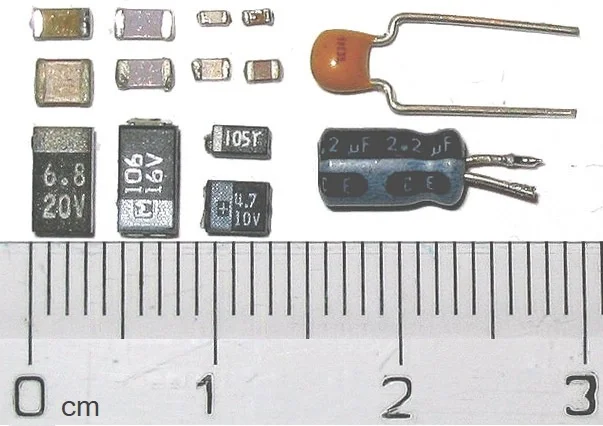
The photograph shows capacitors for scale, not the example resistor.
The relevant original manufacturer documents include Panasonic’s ERJ type datasheet, dated 29 May 2025, and Surface Mount Resistors Land Pattern, dated 24 December 2025. Record the revisions used for the project and check for updates before release.
This resistor is an example, not a proxy for every 0201 part. A capacitor, inductor or another resistor series can have different terminals, mounting recommendations and electrical constraints even when its body belongs to the same nominal size class.
Compare the recommended lands with the board—not just the library
Panasonic’s Surface Mount Resistors Land Pattern document provides an example for the rectangular 0603 metric / 0201 inch resistor family. In its diagram:
| Dimension | Meaning | Panasonic example |
|---|---|---|
| a | Gap between lands | 0.30–0.40 mm |
| b | Overall outside span of the lands | 0.80–0.90 mm |
| c | Land width | 0.25–0.35 mm |
These are manufacturer recommendations for the relevant family, not universal 0201 values. They also do not by themselves specify the stencil apertures or prove that a particular PCB can be assembled.
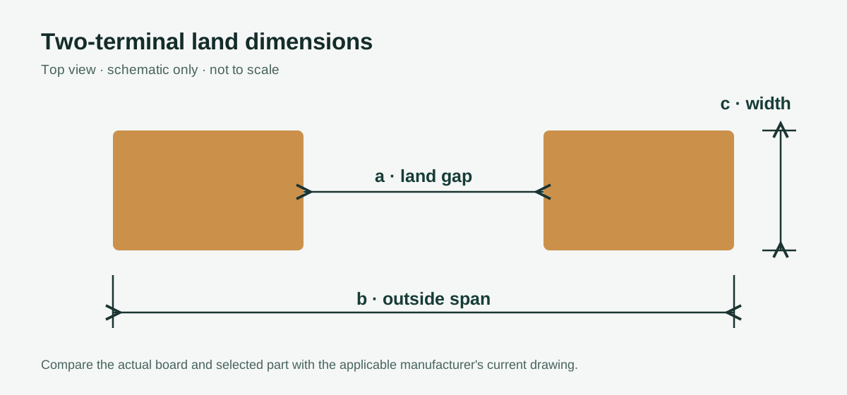
The dimension labels identify what to compare; the drawing is schematic and is not a manufacturing template.
For ERJ1RHD1001C, the designer should compare the actual CAD footprint and fabrication outputs with the manufacturer diagram, including the dimension definitions and units. Then the fabricator and assembler should review what will actually be produced:
- Copper land shape, gap and width, including fabrication tolerances.
- Solder-mask openings and any mask separation or registration concerns.
- Traces and copper connected to each end, including potential thermal imbalance.
- Nearby components, markings and other features that constrain printing, placement or inspection.
- The relationship between the copper, mask, paste-layer and assembly drawings.
The IPC-7351 land-pattern standard can inform the design method, but a general standard or library name is not a substitute for checking this part and board.
Worked example: check a proposed footprint
Assume a designer proposes two identical rectangular lands, each 0.25 mm long by 0.30 mm wide, separated by 0.35 mm. These are hypothetical CAD dimensions, not measurements from a manufactured board. For this illustration, compare them with the Panasonic rectangular-family example above:
| Check | Hypothetical CAD value | Panasonic example | Result |
|---|---|---|---|
| Gap, a | 0.35 mm | 0.30–0.40 mm | Within the example range |
| Outside span, b | 0.25 + 0.35 + 0.25 = 0.85 mm | 0.80–0.90 mm | Within the example range |
| Land width, c | 0.30 mm | 0.25–0.35 mm | Within the example range |
This comparison clears only the nominal CAD dimension check. It does not establish finished copper dimensions, mask registration, paste release, thermal balance or inspection coverage. The designer still needs the actual board files and tolerances; the fabricator and assembler must review the proposed build and its first-article evidence before production release. If any check is missing, the decision remains conditional.
Release-risk matrix
Use the matrix as a decision record, not a scoring system. Stop means a required input or decision is missing; conditional means the proposed method needs agreed verification; release means the named evidence has been reviewed for this build.
| Decision gate | Stop or conditional trigger | Evidence needed for release | Accountable decision |
|---|---|---|---|
| Part identity | Bare “0201,” incomplete MPN or unapproved alternate | Manufacturer, full MPN, size system, dimensions and electrical requirements | Designer approves BOM |
| Board interface | Footprint or mask output not checked against the selected part | Land comparison plus fabricator and assembler review of actual outputs | Designer approves design; fabricator confirms producibility |
| Paste deposit | Aperture, stencil or paste plan is unspecified | Board-specific stencil data, paste information and print verification plan | Assembler approves print process with designer review where needed |
| Placement | Tape presentation, coordinates or machine setup unresolved | Reconciled program, part presentation and first-article placement check | Assembler approves setup; designer resolves data conflicts |
| Reflow and tombstoning | Profile or asymmetry concerns remain untested | Measured profile, component limits and agreed defect response | Assembler approves process; designer approves design changes |
| Inspection and function | Coverage or acceptance criteria are undefined | Method, scope, limits, electrical tests and records | Customer/product owner accepts coverage; assembler executes agreed checks |
| Product life | Production samples are treated as lifetime proof | Product-specific qualification plan and results | Product owner approves qualification |
Clearing one gate does not clear the others. In particular, a manufacturable footprint does not establish electrical performance, and an attractive solder joint does not establish service life.
Turn the BOM and part presentation into controlled inputs
The BOM should identify the manufacturer and complete MPN, not just value and “0201.” Include the required electrical characteristics, approved quantity per board, reference designators, revision and any do-not-populate positions. Reconcile it with the assembly drawing and placement file.
For this Panasonic example, do not plan to read the value from the component after placement: the ERJ datasheet indicates that these small sizes are unmarked. Identification instead depends on controlled part receipt, reel labeling, setup verification and traceability.
Ask the assembler how the supplied quantity will be presented. Tape orientation, reel or cut-tape condition, usable leader, pickup setup and expected setup consumption can affect whether the ordered material is usable. Agree any extra material quantity for the actual build rather than inventing a universal allowance.
An alternate part needs explicit approval. Even if its electrical value and nominal size match, compare its dimensions, terminal construction, recommended lands, packaging and process limits. Decide whether the change requires another stencil review, first article or product test.
Validate paste release and placement together
Panasonic’s checked ERJ1R documents do not give a universal stencil thickness, aperture reduction or paste volume for this part. The assembler therefore needs to review the actual paste-layer data and propose a stencil for this board and process.
That review should identify the aperture shape and dimensions for each land, stencil thickness, fabrication method, registration assumptions and paste alloy/type. Consider whether the selected apertures can release paste consistently with the proposed stencil and printing process, especially alongside other component types on the board. Inspect the resulting deposits for volume and balance rather than assuming that matching an aperture to a pad guarantees a good print.
See SMT stencil design for the broader design context. The output for this build should be a revision-controlled stencil file and an agreed print verification plan—not a copied 0201 recipe.
Placement needs the same board-specific treatment. Reconcile the BOM, footprint origin, coordinates, rotation convention, board side and assembly drawing. The Panasonic datasheet calls for observing the resistor’s front/back orientation as presented in tape. The assembler should confirm the actual feeder, nozzle, pickup and placement setup and check a first article for presence and alignment.
The checked manufacturer material does not establish a universal placement offset, force or machine-accuracy limit. If the assembler proposes limits, record their basis and how compliance will be checked for this job.
Reflow and tombstoning: verify the combination
Tombstoning is a release risk because the two ends of a small passive may not experience balanced solder wetting and heating. Land geometry, copper connections, paste deposits, placement and reflow can all matter. Panasonic’s Technical Guide Ver.3 discusses its “manhattan phenomenon” in connection with common lands and excess solder, including separation by solder resist.
The practical decision is to review both ends of each relevant footprint and then validate the assembled result. Do not claim that symmetric-looking pads alone eliminate tombstoning. For broader defect analysis, see PCB tombstoning causes and prevention.
The assembler should propose a reflow profile compatible with the selected paste, board and all components. Measure temperatures at agreed representative board and component-terminal locations, including potentially different thermal environments. Compare the results with the applicable component limits.
Panasonic publishes conditional recommended soldering information for its rectangular resistor family in Surface Mount Resistors Recommended Soldering Conditions. Its documentation distinguishes protection of resistor characteristics from establishing stable soldering conditions. A manufacturer profile is therefore an input to the review, not proof that the production board will solder reliably. Record the approved profile, measurement locations, deviations and rework or repeat-reflow restrictions applicable to the complete assembly.
Specify what inspection and verification can actually see
The RFQ should separate process inspection, electrical verification and product qualification:
- SPI, if used, can provide evidence about accessible printed deposits under the agreed program and limits. Define which deposits are measured, what characteristics are evaluated and what happens after an out-of-limit result.
- AOI, if used, can check programmed, visible features such as presence, alignment or solder appearance within the system’s validated coverage. Ask which features are not reliably visible and how they will be handled. Do not assume every solder-joint feature can be judged from an image.
- Electrical test needs a defined list of functions, nets or values, access method and coverage. A visual check cannot establish the value of an unmarked resistor.
- Product qualification addresses the intended environment and lifetime through a plan owned by the product organization. Its scope depends on the application.
Agree the applicable customer drawing or acceptance criteria, inspection and sampling scope, defect disposition, rework authorization and records. A pass at SPI, AOI or a sample inspection does not prove electrical function or lifetime. Likewise, a sample pass says nothing automatically about unsampled boards.
Hypothetical quantity and sample reconciliation
Suppose an order starts with 30 panels of four board positions each:
- Total positions: 30 × 4 = 120 boards.
- Four boards are scrapped during depaneling: 120 − 4 = 116 remain.
- Twelve of those 116 are selected for a specified sample examination. The other 116 − 12 = 104 are outside that sample.
- Two sampled boards are consumed by destructive examination. If the other ten sampled boards are eligible to return to inventory, the potential remaining quantity is 104 + 10 = 114.
This is a material reconciliation, not an acceptance rate or a yield claim. It does not say the 104 unsampled boards passed the sample examination, that the ten returned boards are electrically good, or that 114 boards are authorized to ship. The parties must separately agree the sample locations, references examined, test coverage, disposition and required deliverable quantity.
RFQ and release checklist
Send an RFQ with the board revision, intended quantities and schedule through the assembler’s agreed process or request a quote. Assign each item an owner before ordering:
- Designer — approve the part and layout: supply the BOM with full MPNs, manufacturer documents, approved alternatives, electrical requirements, footprint source and comparison to recommended lands.
- Designer — release consistent files: provide fabrication outputs, mask and paste data, assembly drawings, coordinates, board outline, panel details and revision identifiers. Resolve discrepancies before manufacture.
- Fabricator — confirm the actual board proposal: review copper and mask features, tolerances, panelization and any exceptions that affect the lands or assembly.
- Assembler — propose the process: identify part presentation requirements, stencil and aperture data, paste, placement setup, reflow verification, inspection methods and limits. Flag unresolved assumptions rather than presenting a generic 0201 capability.
- Designer and assembler — disposition the first article: agree what will be measured, the acceptance basis, who may authorize changes and whether a changed footprint, part, stencil or process requires revalidation.
- Customer or product owner — accept coverage: define electrical testing, sample and destructive-test scope, traceability, quantity reconciliation and product qualification responsibilities.
- Release authority — sign the revision: confirm that open deviations are accepted or closed and that the approved files, process and evidence refer to the same board and BOM revision.
If the actual footprint, stencil proposal, measured process evidence or acceptance plan is still unavailable, keep the decision conditional. The first release can be for a controlled prototype or process-verification build rather than unrestricted production.
Is 0201 imperial the same as 0201 metric?
No. Imperial 0201 corresponds to the 0603 metric class, approximately 0.6 × 0.3 mm. Metric 0201 is the much smaller 008004 imperial class. State the naming system and check the selected part’s actual dimensions.
Can an 0201 capacitor use the Panasonic resistor lands above?
Do not assume so. Check the capacitor manufacturer’s recommendation and the actual board and assembly process. The Panasonic example is for the applicable rectangular resistor family, not every passive with a similar body size.
Does a smaller body guarantee a smaller PCB?
No. Compare the complete land pattern, clearances, mask, routing and assembly access. The body outline alone does not determine the usable layout area.
Does AOI or SPI replace electrical testing?
No. These methods provide defined process or visual evidence within their coverage; they do not prove circuit function or product lifetime. Agree electrical tests and qualification separately.
What should happen if the assembler proposes an alternate part or stencil?
Hold the change for review. The designer should approve any part substitution, and the assembler should document the revised process. Together, decide which footprint, print, placement, reflow, inspection and product tests must be repeated.