
What engineering teams prioritize first when routing 112G SerDes channels
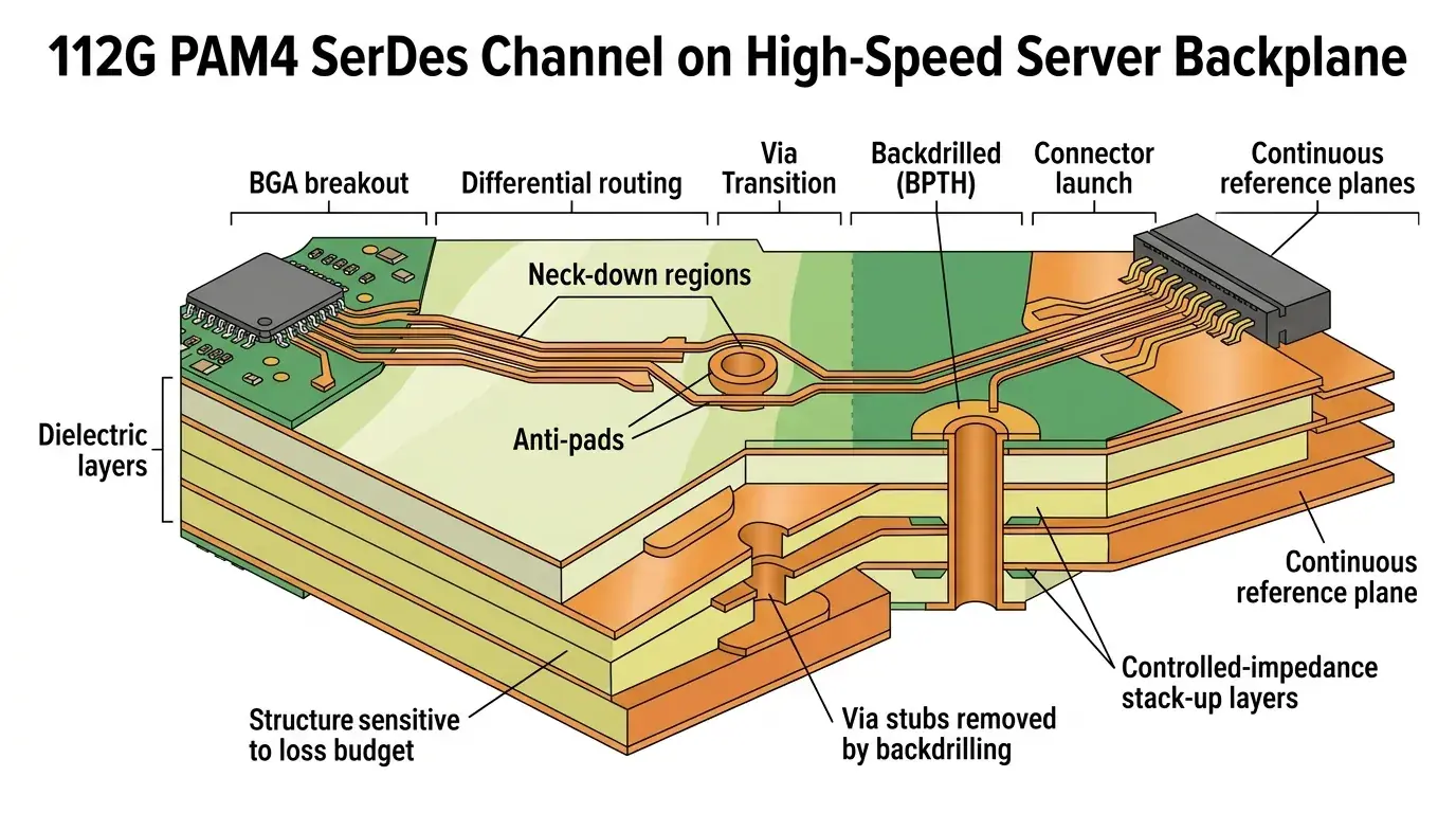
When routing 112G SerDes channels, engineering teams typically do not prioritize the length of individual traces first, but instead focus on the allocation of the overall channel budget, critical structural transitions and realistic manufacturing tolerance windows. For AI servers, switches, accelerator cards and platforms based on ultra-high-speed modules, the true determinants of first-prototype success are BGA fanout, via transitions, backdrilling, connector characteristics and stackup materials. Many projects show delays precisely because risks emerge late — not at the center of the longest traces, but at these critical transition points.
Validation Index
- Where are margins lost first in a 112G channel budget?
- Why do BGA fanout and via transitions erode margins at 112G?
- Why must backdrilling strategies precede layout completion?
- How stackup, materials and copper roughness jointly affect losses
- Why connector launches and reference planes must be examined together
- Establishing closed-loop DFM validation cycles for 112G channels
- Frequently Asked Questions (FAQ)
- Next steps: Initiating pre-engineering and 112G channel validation
Overview of DFM review in 112G SerDes routing
| Risk Dimension | Public Reference / Standard | DFM / SI Design Focus | Engineering Reminder |
|---|---|---|---|
| Data Rate and Margin | 112G PAM4 corresponds to approximately 56 GBd; the Nyquist frequency is ~`28 GHz` |
The budget must explicitly split the contributions of package, traces, vias and connectors. | Create a link budget breakdown before routing. |
| Via and Stub Risk | High-frequency channels require minimal stub control. | Backdrill requirements, stub windows and forbidden zones must align with the real layer structure. | Freeze the backdrilling strategy early. |
| Stackup and Materials | Long runs depend critically on low-loss substrates and stable laminations. | Consider resin system, foil roughness for laminations consistent with impedance. | Tie material selection to lamination stability. |
| Validation Cycle | TDR, S-parameters and measured correlations define high-speed SI standards. | Simulations, coupons and tests must close into an empirical validation loop. | SI validation depends on sample reliability and repeatability. |
Where are margins lost first in a 112G channel budget?
Within a 112G design, the first deductions from the signal budget rarely depend only on the longest trace, but often on the cumulative effect of multiple structural anomalies, local reflections and modal conversions. In 112G PAM4 runs, without thorough mapping, teams may incorrectly infer adequate headroom because they judge the path as "short", underestimating how quickly discrepancies in BGA fanout and layer changes have already compromised the margin.
Public technical documents place the discussion of 112G PAM4 channels at Nyquist frequencies around 28 GHz and baud limits of 56 GBd (e.g. OIF CEI-112G). On server-class boards, attenuation criticalities emerge here:
- Breakout area and BGA fanout (trace neck-downs, anti-pad clearances, etc.).
- Internal transitions and imbalances arising from via stubs.
- Connection discontinuities near launches and high-density sockets.
- Deviation from calculated losses due to dielectric absorption or deep copper roughness on medium and long runs.
- Reference plane interruptions and loops induced by isolation for mounting or overly compressed routing.
Therefore, proceeding correctly in a 112G design means first decomposing the budgets for package, via transitions and connector launch zones, determining what to lock down from the very start of strategy definition.
Why do BGA fanout and via transitions erode margins at 112G?
BGA breakout and via transitions consume a disproportionate share of 112G SerDes margins because they concentrate delicate steps: drastic width variations, layer jumps onto split references and discontinuous control of characteristic impedance. They physically span only a few millimeters, but the losses and frequency conversions they cause are unforgiving.
To correctly apply the routing rules for 112G SerDes channels, the team's technical reviews must focus on verifying that:
- Breakout patterns do not demand excessive reductions (extreme neck-downs) or redundant layer hopping.
- Via diameters and clearance tolerances respect centering with the impedance of the local dielectric.
- Iterative accumulation of transitions through passing vias between different layers is avoided.
- Tolerances on final plating, drill hole sizing and layer offsets coincide with a real and sustainable factory DFM parameter.
- The overall effect of structural discontinuities in the footprint area has been co-simulated considering package models.
The deviation of performance on physical PCBs from simulated results rarely stems from tool bugs, but rather from the failure to insert these "ideal" points into the analytical equations with the correct manufacturing tolerances. Models and industry standards (e.g. OIF-CEI-05.3) reiterate the destructive impact of these short but unstable discontinuities.
Why must backdrilling strategies precede layout completion?
Implementing backdrilling after closing the routing is not a sound option in 112G designs, precisely because a partial drill structurally modifies the residual stub resonance line and is tied to cumulative tolerances. A statement on the final files does not work miracles: if the layers, depth, stub residual and copper-free space have not been determined, emissions and path integrity remain at high risk.
Working within architectures governed by backdrill process rules, risk containment requires that:
- Acceptable loss parameters are defined by evaluating the total panel thickness and the operational layers.
- There is an exact delimitation of the paths that constrain blind drilling operations and those considered insensitive for which a through via suffices.
- Defined depths, anticipated DFM tolerances and physical limits flow into the release documents (stackup/drill plan).
- There is consistency at the interfaces with the surrounding plane (anti-pad dimensioning).
- Local impedance coupons demonstrate, during first-article fabrication, that the rules and CNC machines have passed setup.
In short, including backdrilling means triggering a decision that critically concerns the SI leads and the CAM managers of the PCB firm — it is not admissible to fold it back onto itself after layout delivery.
How stackup, materials and copper roughness jointly affect losses
The loss profile at 112G represents a balance that combines an integration of the stackup's structural architecture with the thermal absorption of dielectric resins and the typical roughness of the copper foil surface due to skin effect. Near 28 GHz, ignoring an unstable mix or the physical alteration determined by the pressing operation in the lamination process risks diverging completely from the datasheet promises.
For those analyzing high-speed budget and stackup for 112G SerDes, verification is recommended of:
- The tangency to maximum deterioration limits of the mid or low-loss material type, as a function of the routing on the scheme.
- Matching resin families to the operational limits guaranteed by the high-speed PCB services in factory.
- Qualifying how different treatments (HVLP, RTF) will directly affect the deviation from ideal conduction at high power.
- The influence of the glass-resin matrix on homogeneous distribution, the cause of micro-impedance shifts and intra-skew in adjacent layers.
- The consistency and quantitative traceability both in the supply chain for large volumes and for the first analyses.
A robust combination of low-loss material goes beyond "face values": it requires guaranteeing stable insertion windows even across standard series variations without exceeding the budget. Not coincidentally, the assumptions underlying the IPC-6012 Endorsement Program protocols also confirm the goal centered on real reliability in rigid panels.
Why connector launches and reference planes must be examined together
Inspecting the patterns dedicated to injecting ultra-high frequency into connectors while ignoring the surrounding continuous substrate context is a source of unwanted returns in transfer. Much of the noise is generated not by the physical footprints ascribed to the component, but in reaction to the complex proximity with shield clearance, BGA fanout unevenness and forced changes in the ground current net paths.
Examining advanced multilayer PCB architectures, a proper inspection decision focuses on:
- Updating the density of the launch's adjacent network together with anti-pad calibration.
- Ensuring that for impedance-symmetric paths (differential pairs), routing proceeds in parallel without stumbling over ground fractures or shared areas.
- Surveying drilled cuts, thermal vias, unplated slots that prevent perfect closures of reference flows.
- Synoptic integration at the hardware installation point interfacing with package via conversion.
- Complete extraction of the architecture in SI Full-Wave, simulating the dimensional deviation in the planes pre and post assembly at high impedance.
Many chains fail when "the distances looked good", due to the abrupt isolation that arises precisely at the final junction at the connector entry.
Establishing closed-loop DFM validation cycles for 112G channels
The real verification for a DFM-oriented SerDes PAM4 project coincides with the adoption of preventive measures attested by first-build yields: a test based on data and feedback rather than segmentation of the working pipeline. Bring-up functionality tests do not exclude a retroactive and combined tracking of controlled drilling limits and the chemical and impedance repeatability on dedicated test coupons, guaranteed within a continuous validation cycle.
Ideal audits cover:
- Structural Substrate Management: Fixing material families, copper weights and dielectric substrates bound by controlled impedance ranges integrable with measurable coupon positions.
- Transverse Definition Across Drilling & Stubs: Assigning nets destined solely for hole countersinking and the correct advancement tolerances on the DFM chip depth.
- Joint Approach to Connector Breakout: Examining on dual frequency the interconnected via component in combination with integrity verification protected by physical shielding in the gerber release phase.
- Validation with S-Parameter and TDR-Sweep: Tests on raw files and correlations between bare single board and component installed in high applied density.
- Final Handoff Set: Homogeneous archiving framed between criteria issued in the Stackup Extraction Guide, the methodologies tied to Gerber File Generation, and in harmony with the Integrity for PCB design release packages.
- Reliability Mapping Across Batches: Planting cross matrices for testing on componentry and the Reliability on physical tests during multichannel contracts.
An engineering effort deprived of the test/verify loop will drag through perpetual and exhausting cycles aimed at recovering, retouching and re-supplying pre-series before a stable line even assures volume yields and expected ROI.
Frequently Asked Questions (FAQ)
Q: Is there a non-negotiable constraint on using ultra-low loss resins and cores on 112G boards?
A: Absolutely not in total. The technological step must accompany balances for overall net lengths, the number of relay components, TX/RX chip isolation quality and adequate monetary resources for the run in question. Often a medium-loss material class returns sufficient marginality in direct links if accompanied by robust SI calculations, but it is not worth assuming it as a cold estimate without physical control of the margins absorbed at the bench.
Q: Do you consider backdrill operations always necessary whenever the 112G PAM4 standard surfaces?
A: Not at all. The variables to which identification must be applied remain the raw panel footprint, the network substrate compositions and, by way of extremely high incidence, the destructive magnitude of the fixed-length antenna calculation in the field return at the point (resonance reflection) of the stub not employed by the link. Establish stringent selection rules rather than generic summary applicability.
Q: If the traced differential channels respond scrupulously to the same length, have I placed the 112G system in total passive safety operation?
A: Length matching does not at all qualify high-bandwidth channels such as streaming at 112G. Above that, true fracture points are determined by asymmetries and parasitic overlaps at the start of the package frame (BGA), distortions tied to deep aperture in back vias and a localized distortion at the insertion and soldering footprints on the exterior.
Q: Where does the entire gap between a successful software engineering check and a systemic alarm during pre-production hardware analyses on an ultra-high-density integrated board (Bring Up) originate?
A: Large discrepancies always draw their nature from the manufacturing tolerance omitted by the simulator software conceptually, such as the incisiveness of abrasion at high frequencies tied to the chemical finish used or slight deviations of the stamp and positioning. All deviations precluded by validation tests if the factory's predefined empirical inspection parameters on separate coupons for controlled impedance do not enter into the extracted calculations.
Q: Critical blocking elements that must be "sealed" prior to the definitive CAM release of an order on a 112G SerDes board?
A: Categorically close matrices in the loss budget defined for system and layer use. Confirm integral plans on the stack of dielectrics to be used including HV sheets, determining strict limitations on CNC backdrill and relative profiles and splits of the antenna return, as well as establishing analytical plans for inspection on differentiated coupons post release in TDR limit test.
Next steps: Initiating pre-engineering and 112G channel validation
If a technical team is building modules, optical arrays or data servers with a backbone set toward PAM4 / 112G SerDes, the question is not to ask online limiting oneself to "whether or not you possess the certification to supply them", but to immediately set up solid preventive engineered workflows sheltered from the classic deficits. It is advisable to prepare for verification:
- Gerber plans together with the corresponding ODB++ models, implemented with calculation sheets on the stackup defined by impedance.
- Zoning (Package VS Internal Tracing VS Launches) and etching elaborations for heavy components in backdrill or convert arrays.
- Coupons for TDR parameter detection in SI to be set up in matrix form.
Sharing them alongside the library for Routing limits in 112G and the calibration to the baseline documentation on absorption calculation in layers for SerDes budget, on the concrete HDI setup and High-Speed assembly production options paired with the base frameworks on advanced systems of precision in Backdrill process capabilities differentiates careless empirical indications from the real competencies that guide an R&D cycle to volume production mass-market.
To receive a DFM review or activate preventive procedures regarding adaptation on SerDes channels and margin feasibility on the substrates to be inserted in the lot, contact the PCB engineering staff directly.
Extended Documentation and DFM Guidelines:
- DFM Restrictions on 112G SerDes Routing
- Budget Allocations for Stackup at 112G PAM4 Frequencies
- Overview of Advantages and Processes in Backdrill Tolerance
- Gerber Data Export Requirements and Guidelines
- Delivery Standards and Production Handoff on Sensitive Circuits
*Author: HILPCB High-Speed Interconnect Engineering Team* *Review approved by: HILPCB SI/DFM Engineering Team* *Last updated: 2026-04-01*