
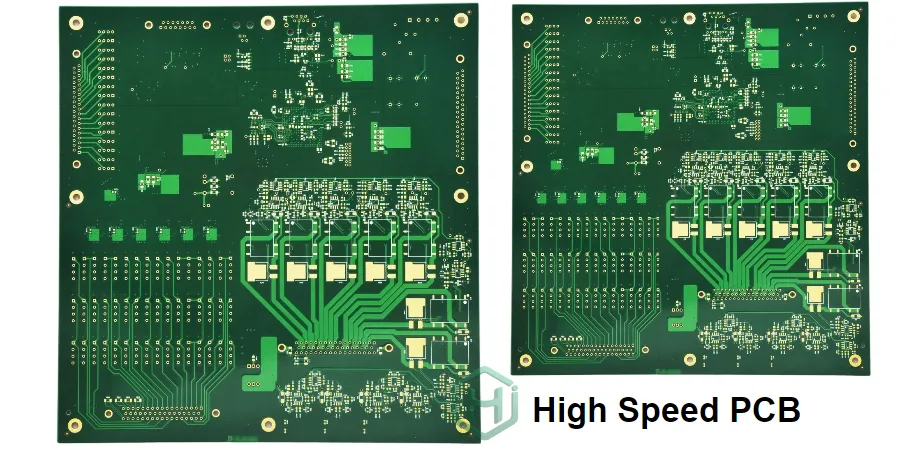
With explosive bandwidth demand from data centers, AI, and 5G communications, data rates have entered the 112Gbps/s era. In this context, 112G SerDes technology has become a core enabler for next-generation high-speed interconnect. But at this speed, PCB design and manufacturing face unprecedented challenges. A well-designed 112G SerDes routing stackup is no longer “just lamination”; it is systems engineering that combines materials science, electromagnetic theory, and precision fabrication. It directly determines signal integrity, link stability, and ultimately product success.
This article serves as a detailed 112G SerDes routing guide from the viewpoint of connector and via-transition design. We cover everything from channel budget and material selection to manufacturability, helping you navigate this complex space. For teams building cutting-edge high-speed PCB, mastering an optimized 112G SerDes routing stackup is a prerequisite for success. Highleap PCB Factory (HILPCB) leverages deep high-speed experience to support customers from prototype through volume.
Why is the 112G SerDes channel budget so strict?
In 112G SerDes design, everything starts with Channel Budget. The channel budget defines the maximum allowable signal loss and noise margin across the physical link from transmitter (Tx) to receiver (Rx). Compared with earlier generations (28G/56G), the 112G budget is extremely tight—primarily because it uses PAM4 signaling.
PAM4 carries 2 bits per symbol, halving the baud rate and easing some bandwidth pressure, but it reduces SNR by ~9.5dB and dramatically increases sensitivity to noise and attenuation. The Nyquist frequency of 112G PAM4 reaches 28 GHz. At this frequency, PCB traces, vias, and connectors introduce significant Insertion Loss (IL).
A typical 112G channel includes multiple parts, each consuming precious loss budget:
- ASIC package: Substrate traces and vias in the BGA package are the first loss contributors.
- PCB traces: The primary loss source—driven by dielectric loss, conductor loss (skin effect and copper roughness), and trace length.
- Vias: Through/blind/buried vias are major impedance discontinuities that add reflection and extra loss, especially on large backplane PCB.
- Connectors: High-speed connectors such as QSFP-DD and OSFP must be precisely modeled, including the PCB launch region.
- Cable assembly (optional): In rack-to-rack interconnect, the cable and its connectors are also part of the channel.
Total channel insertion loss is typically constrained to ~30–35dB (@28GHz). Excess loss at any single element can prevent link bring-up or push BER out of spec. Therefore, accurate channel modeling and budget allocation is the first—and most critical—step in 112G SerDes routing stackup design.
How do you choose the right low-loss materials?
Material selection is the foundation of low-loss 112G SerDes routing. At 28GHz, traditional FR-4 loss is unacceptable, so low-loss or ultra-low-loss laminates designed for high-speed applications are required. The core metrics are Dk and Df.
- Dk: Impacts propagation speed and characteristic impedance. In high-speed design, you want stable Dk across frequency to reduce dispersion. Lower Dk also enables wider traces, helping reduce conductor loss.
- Df: Directly quantifies dielectric loss. For 112G SerDes, Df at 28GHz should be below 0.004—often closer to 0.002.
Beyond Dk/Df, two additional factors matter just as much:
Fiber Weave Effect: The periodic structure of fiberglass weave creates local Dk non-uniformity. When trace length becomes comparable to the weave pitch, impedance variation and skew can degrade differential signaling. Common mitigations:
- Use flatter glass styles (e.g., 1078, 1067).
- Use Mechanically Spread Glass.
- Route at a slight angle (e.g., 1–5°) relative to the weave to avoid parallel alignment.
Copper Roughness: At high frequency, skin effect forces current to the conductor surface. Rough copper increases effective path length and conductor loss. Use very smooth copper such as VLP or ULP; typical Rq should be below 2 µm.
High-speed PCB material performance comparison
| Material class | Typical Dk (@10GHz) | Typical Df (@10GHz) | Target data rate | Cost index |
|---|---|---|---|---|
| Standard FR-4 | 4.2 - 4.8 | 0.015 - 0.020 | < 5 Gbps | 1x |
| Mid-loss materials | 3.6 - 4.0 | 0.008 - 0.012 | 10 - 28 Gbps | 2x - 3x |
| Low-loss (e.g., Megtron 6) | 3.2 - 3.6 | 0.002 - 0.004 | 28 - 112 Gbps | 5x - 8x |
| Ultra-low-loss (e.g., Tachyon 100G) | < 3.0 | < 0.002 | 112 Gbps and above | > 10x |
What are the key strategies for impedance control and crosstalk management?
In 112G SerDes routing stackup, precise impedance control and strict crosstalk suppression are two more pillars of signal quality.
Impedance control: Differential impedance is typically 100Ω or 90Ω, with tolerance as tight as ±7% or even ±5%. Any geometric deviation from target impedance causes reflections, increasing insertion loss and jitter. Key factors include:
- Trace width and thickness: Etch accuracy in manufacturing determines final linewidth.
- Dielectric thickness: Post-lamination PP (Prepreg) thickness control is critical.
- Material Dk: Simulation must use Dk provided by the laminate supplier that accounts for resin content and lamination conditions.
Crosstalk management: Crosstalk is noise caused by EM coupling between adjacent traces. In 112G PAM4 systems where SNR is already low, crosstalk is often the #1 killer. Common strategies:
- Increase spacing: Differential-pair-to-pair spacing is often recommended at 3W or more; on critical links, 5W or wider may be needed.
- Reference-plane continuity: Ensure continuous reference GND/power planes under high-speed routing; avoid crossing plane splits.
- Orthogonal routing between adjacent signal layers: Route directions should be perpendicular to minimize broadside coupling.
- Ground-via shielding: Place Stitching Vias strategically around differential pairs to form a Faraday-cage effect and isolate noise.
Effective crosstalk control must start at the stackup planning stage, using 3D full-wave EM simulators (e.g., Ansys HFSS, CST) for accurate prediction and optimization.
How important is transition optimization for connectors and vias?
As a connector and via-transition design specialist, I can say confidently: at 112G, transition design quality directly sets the upper limit of channel performance. An unoptimized via or connector pad can easily consume several dB of budget via loss and reflection.
Via optimization: A via is a complex 3D structure. Its parasitic capacitance and inductance create severe impedance discontinuities at 28GHz. Key tactics include:
- Back-drilling: One of the most important techniques. By drilling out the unused via Stub from the backside, you remove quarter-wavelength resonances and significantly improve insertion loss and reflection. Backdrill depth control is a key indicator of a manufacturer’s capability.
- Anti-pad optimization: Increasing the Anti-pad opening in reference planes reduces via parasitic capacitance and brings impedance closer to the transmission line.
- Remove NFP: Removing Non-Functional Pads on inner layers reduces parasitic capacitance and further improves performance.
- Use HDI PCB technology: Microvias and smaller pads reduce physical via size and parasitic effects dramatically.
- Ground-via co-design: Place 1–2 rings of ground vias closely around the signal via to provide a low-inductance return path and suppress coupling.
Connector optimization (Launch Tuning): High-speed connector pin arrays (e.g., QSFP-DD) are extremely dense, making pad and fan-out design challenging. You must run 3D simulation to fine-tune pad shapes, trace widths, and reference-plane openings to match connector impedance and achieve a smooth transition.
🧬 Via transitions: an optimization matrix for high-speed vertical links
Eliminate impedance jumps and parasitics to protect 112G+ signal integrity
Execution standard: Remove via stubs completely to eliminate resonance points at high frequency. For data rates above 28Gbps, keep stub length strictly within < 10 mil to maintain bandwidth linearity.
Execution standard: Remove unnecessary inner-layer pads across layers. Reducing parasitic capacitance improves overall TDR behavior and lowers reflection at the via transition.
Execution standard: Use a 3D full-wave solver to optimize Anti-pad dimensions. Fine-tune via-to-plane spacing to compensate local inductance and ensure impedance continuity through the vertical transition.
Execution standard: Place GND Stitching Vias symmetrically around signal vias to form a coaxial-like return path, isolating via crosstalk and reducing return-loop inductance.
Fine-tune the fanout region for a specific connector (e.g., QSFP-DD or PCIE 6.0). By adjusting pad edges and lamination gaps to the reference plane, ensure a smooth transition impedance from horizontal routing to the vertical connector and minimize Total Insertion Loss.
How do equalization and jitter affect SerDes link performance?
Even with an optimized 112G SerDes routing stackup, channel loss still exists. Modern SerDes devices include powerful Equalization circuits to compensate. Common equalization blocks include:
- Tx FFE: Pre-emphasis boosts high-frequency components to counter the channel’s low-pass behavior.
- Rx CTLE: A programmable amplifier that selectively boosts high-frequency content to flatten channel response.
- Rx DFE: A nonlinear equalizer that cancels ISI from previous symbols.
The PCB’s goal is to provide a “smooth and predictable” channel. A channel response full of resonances and abrupt discontinuities makes equalizers hard to converge—or may cause failure.
Jitter is time-domain deviation and another major enemy of high-speed links. PCB-side jitter sources include:
- Fiber weave effects in the material.
- Reflections from impedance discontinuities.
- Power Supply Noise: PDN noise couples through SerDes power pins into the signal and creates jitter—highlighting the importance of co-design across SI and PI.
A robust stackup reduces jitter and ISI at the physical layer, lowering reliance on SerDes equalization and improving overall 112G SerDes routing reliability.
How does DFM balance performance and cost?
A theoretically perfect 112G SerDes routing stackup is meaningless if it cannot be manufactured economically and reliably. DFM must be considered early. HILPCB engineers emphasize early involvement to help customers avoid manufacturability traps.
Key DFM considerations include:
- Line width/spacing control: 112G designs often require 3/3mil (~75/75μm) or finer, placing high demands on imaging and etching.
- Drilling accuracy: High layer count and high Aspect Ratio PCBs demand very high alignment accuracy in mechanical and laser drilling.
- Backdrill depth control: Backdrill depth tolerance directly affects stub length and requires advanced Z-axis control equipment.
- Stackup symmetry: To reduce lamination warpage, keep the stackup as symmetric as possible.
- Surface finish: For 28GHz, ENEPIG often outperforms ENIG due to better flatness, corrosion resistance, and skin-effect behavior.
In early phases—especially when you need 112G SerDes routing quick turn—close collaboration with an advanced manufacturer and DFM review helps avoid late, expensive redesign and accelerates time to market.
HILPCB high-speed PCB manufacturing capability overview
| Process parameter | Capability |
|---|---|
| Max layer count | 64 layers |
| Min line width/spacing | 2.5 / 2.5 mil |
| Max Aspect Ratio | 20:1 |
| Backdrill depth tolerance | +/- 2 mil (50μm) |
| Impedance control tolerance | ±5% |
How do you ensure long-term reliability for 112G SerDes routing?
112G SerDes routing reliability includes not only meeting electrical targets, but stable operation across product life. Key considerations:
- Thermal management: 112G SerDes devices and optical modules dissipate significant power; stackup design must provide effective heat paths. Adding thermal reference planes, using materials with better thermal conductivity, and strategically placing Thermal Vias help control device temperature and prevent performance drop or permanent damage.
- Power Integrity (PI): A low-impedance, stable PDN is foundational. Proper decoupling placement, wide power planes, and low-inductance via design suppress supply noise and provide “clean power” for SerDes.
- CAF resistance: In high-density PCBs with high electric-field gradients, CAF is a potential failure mode. Selecting high-CAF-resistance materials and using optimized drilling/plating processes is essential.
- Consistency testing: For volume production, build strict test flows—sample characteristic impedance with TDR and measure S-parameters with VNA to ensure lot-to-lot consistency.
How does HILPCB support low-volume and quick-turn prototypes?
We understand that fast iteration and prototype validation are critical for cutting-edge 112G SerDes development. Many projects start with 112G SerDes routing low volume needs. HILPCB built a flexible production system to support everything from a few prototypes to full-scale volume. How those builds map onto NPI EVT/DVT/PVT stages for high-speed boards is covered separately.
For 112G SerDes routing quick turn projects, we provide:
- Expert DFM support: Free stackup recommendations and DFM analysis before ordering to balance performance and manufacturability.
- Strong material inventory: We stock mainstream low-loss 112G SerDes routing laminates (Isola, Rogers, Panasonic Megtron series, etc.) to avoid long procurement lead time.
- Dedicated prototype line: A rapid-turn line to deliver high-quality high-speed PCBs in the shortest time.
- One-stop service: Beyond PCB fabrication, we support component sourcing and PCBA. Our turnkey assembly can manage the supply chain so you can focus on R&D.
Whether you need 112G SerDes routing low volume validation boards or demanding volume orders, HILPCB has the capability and experience to be a trusted partner.
FAQ
Why is the 112G SerDes channel budget so unforgiving?
Because 112G PAM4 signaling has much tighter noise margin than earlier generations. Loss from packages, traces, vias, connectors, and optional cables accumulates quickly, so a single weak transition can consume too much of the channel budget.
Why are low-loss materials mandatory for 112G routing stackups?
At Nyquist frequencies around 28 GHz, conventional FR-4 introduces too much dielectric loss. Low-loss laminates with stable Dk, low Df, and smoother copper are needed to keep insertion loss and dispersion within a range the SerDes can still equalize.
Why do vias and connector launches matter so much at 112G?
They are major 3D discontinuities in the channel and can create extra reflection, resonance, and loss. Techniques such as back-drilling, anti-pad tuning, and stitched return paths are often necessary to keep transitions usable.
How does manufacturability affect long-term 112G link reliability?
If line width, drilling, backdrill depth, stackup symmetry, and impedance control are not held consistently, the electrical behavior drifts from lot to lot. Reliable 112G performance depends on both good design physics and repeatable manufacturing execution.
Conclusion
Building a robust and reliable 112G SerDes routing stackup is complex systems engineering that requires delicate trade-offs across SI, PI, thermal management, and manufacturing. From strict channel budget analysis, to carefully chosen low-loss materials, to micron-level optimization of vias and connector transitions—every detail matters.
As technology evolves toward 224G and beyond, these principles and challenges will only intensify. Choosing a partner like HILPCB—one that understands both design physics and top-tier manufacturing—can be a decisive advantage. We are not only a manufacturer, but also a companion in technical innovation, turning the most challenging design blueprints into high-performing physical products. If you are launching your next high-speed program and need a reliable 112G SerDes routing stackup solution, contact our technical experts today.