
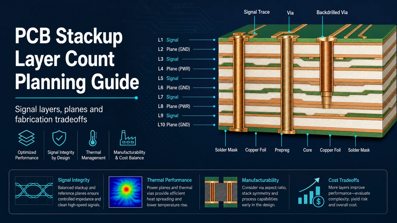
- Start by deciding whether the board is still a baseline single- or double-sided build, or whether it has already crossed into multilayer planning where stackup architecture, reference planes, via strategy, and impedance posture become part of the release burden.
- Layer count is a routing and manufacturability decision, not a default recipe. A 4-layer board and a 24-layer board do not differ only by “more layers”; they carry different planning, validation, and review expectations.
- If high-speed or controlled-impedance nets are part of the design intent, stackup, glass style, material family, coupon ownership, and TDR validation posture need to be reviewed together rather than as separate late-stage notes.
- High-layer designs should be treated as registration-sensitive, lamination-sensitive builds. The right question is not “Can we add layers?” but “What process burden does this layer architecture create before fabrication release?”
- A useful release review freezes the board family, target layer count, stackup branch, material-family direction, and validation ownership before prototype ordering or supplier comparison begins.
PCB stackup and layer count planning is the engineering step that turns a board from a generic layout into a fabrication-ready construction path. The key decision is not the number alone. It is whether the chosen layer architecture matches the board family, routing density, impedance needs, and validation burden the project will carry through release.
In This Guide
- What to review first in PCB stackup and layer count planning
- Early rule table for stackup and layer-count decisions
- How board family and layer count change the planning path
- What goes wrong when layer count becomes a placeholder
- When controlled impedance changes the stackup review
- How validation scope should expand as layer count rises
- Why 16-layer and 24-layer boards need a different release posture
- What to lock before prototype or fabrication release
- FAQ
- Next steps
- References
What to review first in PCB stackup and layer count planning
PCB stackup planning is not the same as picking a layer number from a menu. In engineering review, the first question is which board family the design belongs to, because that determines what has to be planned next.
For rigid boards, single-sided and double-sided designs stay in a baseline low-layer branch. Once a design moves to 4 layers and above, it enters the multilayer branch, where stackup architecture, reference-plane continuity, via planning, and impedance posture become much more important. That boundary matters because it keeps teams from treating a multilayer release as if it were only a slightly busier low-layer board.
The next review is whether the board is still a baseline multilayer build or whether it has already moved into a more demanding branch such as high-speed impedance control, high-layer manufacturability, HDI build-up, or a mixed-material stackup. In practice, that means the layer-count discussion should quickly turn into a routing-path discussion:
- Is this still a straightforward multilayer board, or is stackup architecture now driving the design?
- Do reference planes and return paths need to be protected for controlled-impedance nets?
- Is the selected layer count solving routing density, or is it hiding unresolved branch decisions such as HDI or high-layer registration burden?
- Has the project defined who owns coupon and TDR validation posture if controlled impedance is part of the release?
Useful review at this stage often pairs the design intent with the most relevant HIL path, such as single-double-layer PCB for baseline low-layer work, multilayer PCB when the board clearly sits in the multilayer branch, high-speed PCB when impedance posture drives the stackup, and PCB prototype when the project needs an early release review instead of a generic quote-first discussion.
Early rule table for stackup and layer-count decisions
| Rule or review point | How to judge it early | Why it matters | How to verify | If ignored |
|---|---|---|---|---|
| Board family boundary | Separate baseline single/double-sided boards from 4-layer-and-above multilayer boards | The family split changes what must be reviewed next | Confirm the board family before stackup debate starts | Teams discuss stackup details without first agreeing on the right process branch |
| Layer count purpose | Ask what problem the extra layers solve: routing density, reference continuity, power distribution, or high-speed control | Layer count should solve a real engineering burden, not act as a placeholder | Review net classes, plane needs, and routing congestion together | Added layers hide unresolved design intent and create late release churn |
| Stackup branch | Decide whether the board is baseline multilayer, high-speed impedance-sensitive, high-layer, or another special branch | Each branch carries a different review burden | Align the board with its dominant engineering driver | One generic stackup review tries to cover mismatched problems |
| Reference-plane continuity | Treat plane continuity as part of the stackup decision, not a later routing cleanup | Controlled return paths shape signal behavior and release risk | Review layer transitions and plane changes with critical nets | The board appears routable but is unstable in validation |
| Material-family direction | Keep baseline laminate, high-Tg, or lower-loss direction tied to the stackup branch | Material family affects manufacturability and validation posture | Review the intended use case, especially for higher-layer or high-speed boards | Material decisions are made too late to stay aligned with the stackup |
| Coupon and TDR ownership | Define who owns impedance verification posture if controlled-impedance nets are part of the board | Validation burden belongs in planning, not only after fabrication | Align stackup review with impedance calculator assumptions and release review | The release package assumes impedance control without agreed verification ownership |
If your team already has Gerber data, stackup notes, or an impedance target draft, this is the point to consolidate them before asking for fabrication feedback. A planning review is most useful when layer intent, board family, and validation ownership are still being aligned, not after every assumption has been buried in separate files.
How board family and layer count change the planning path
The most common mistake in stackup discussions is treating all rigid boards as if they were on one continuous scale from “simple” to “complex.” The safer approach is to separate board family identity from stackup architecture.
Single-sided and double-sided rigid boards belong to the baseline low-layer branch. They can still need process review, plated-through-hole attention, and prototype discipline, but they do not automatically carry the same stackup-planning burden as multilayer boards. Once the board reaches 4 layers and above, the planning path changes. At that point, the team should assume that plane structure, via strategy, and layer-role assignment are part of the release question.
That does not mean every multilayer board is a high-layer or high-speed board. It means the board has crossed into a branch where stackup architecture matters enough to deserve early review.
This distinction is especially useful for teams comparing options such as:
- staying with a lower-complexity multilayer architecture versus adding layers to simplify escape routing
- deciding whether routing density really needs a deeper stackup or instead points toward HDI PCB planning
- separating basic power and routing needs from genuine high-speed or controlled-impedance requirements
The layer-count decision is best tied to the board’s dominant engineering burden:
| Situation | Likely planning route | What to decide next |
|---|---|---|
| Baseline low-layer rigid board | Baseline single/double-sided branch | Whether the design still avoids multilayer architecture entirely |
| Ordinary 4-layer-and-above rigid board | Multilayer stackup branch | Plane roles, via strategy, and whether impedance review is needed |
| Routing density pushes beyond ordinary multilayer behavior | HDI or build-up review | Whether density justifies a different interconnect branch |
| High-speed or impedance-sensitive design | Controlled-impedance planning branch | Stackup, glass style, material-family direction, coupon and TDR posture |
| High-layer architecture such as 16-layer or 24-layer builds | High-layer manufacturability branch | Registration burden, lamination-planning intensity, and validation staging |
This is why “What layer count should I use?” is rarely the most useful first question. A better first question is “Which board family and stackup branch is actually driving this design?”
What goes wrong when layer count becomes a placeholder
Teams often add layers for the right reason, but just as often they add layers to postpone a harder decision. That is where stackup planning starts to fail. The problem is not that the board becomes multilayer. The problem is that the extra layers are carrying unresolved architecture.
Several failure patterns appear repeatedly in release review:
- A board adds layers because return paths are broken, but the team still has not defined which layers are the real signal references.
- Routing congestion pushes the design upward in layer count, but the true issue is escape complexity that may belong in an HDI PCB review rather than in a generic multilayer stackup expansion.
- Controlled-impedance nets are added late, so the stackup now carries impedance requirements, but coupon ownership and TDR review are still undefined.
- The board moves toward 16-layer or 24-layer architecture, but material-family direction is still being treated like a purchasing detail instead of part of the manufacturability plan.
- A prototype build is expected to answer too many questions at once: routing fit, high-layer registration sensitivity, signal-integrity posture, and assembly readiness.
These failure chains matter because extra layers can hide branch mistakes for a while. A board may look more routable after another plane pair or signal layer is inserted, but if the design still lacks a stable branch decision, the risk only moves downstream. The release package becomes harder to review, supplier discussions become less precise, and validation starts with blurred objectives.
In practice, layer count should close open architecture questions, not postpone them. If the extra layers are there to stabilize references, separate power domains, reduce routing crossings, or create room for impedance planning, that is a real engineering purpose. If the extra layers are there because the team does not yet know whether the board is baseline multilayer, HDI, high-speed, or high-layer process-sensitive, then the stackup is carrying uncertainty rather than intent.
That is also why high-layer boards should not be judged only by whether they can be fabricated. The more useful review is whether the current layer architecture has a frozen reason:
- Does the chosen layer count solve a known routing-density or plane-continuity problem?
- Does it match the board family and process branch already identified by the team?
- Does it reduce release ambiguity, or does it only make the board look safer while hidden assumptions stay unresolved?
- Does the prototype objective still fit the real question the project needs answered first?
If those answers are unclear, the safest next step is usually not “add two more layers.” It is to reopen the branch decision, review the stackup path with the right product or service route, and make the release burden explicit before the board enters fabrication feedback.
When controlled impedance changes the stackup review
Once controlled-impedance nets are part of the project, stackup planning stops being only about fitting traces and planes onto the board. It becomes a linked decision across geometry, materials, reference structure, and verification posture.
The useful shift is this: controlled impedance should be reviewed as a planning system, not as a number attached to a late fabrication note.
That review usually includes:
- whether the chosen layer architecture gives critical nets stable reference planes
- whether material-family direction and glass style are being considered together with routing intent
- whether neck-downs, layer transitions, and coupling assumptions still make sense within the actual stackup
- whether coupon and TDR ownership is defined early enough to influence release behavior instead of only post-build reporting
Spread-glass planning belongs in this same conversation. For high-speed or skew-sensitive programs, spread-glass selection is not an isolated materials choice. It sits alongside resin system, copper profile, reference stackup, and coupon-based verification posture. The practical implication is that teams should not lock the layer count first and then try to force impedance review into whatever structure remains. The layer architecture and the impedance-validation posture need to be reviewed together.
Natural routing support for this kind of project usually includes high-speed PCB when the board clearly belongs in a signal-integrity-sensitive branch, and multilayer PCB when the stackup still needs broader architecture review before high-speed assumptions are frozen.
How validation scope should expand as layer count rises
One reason stackup planning becomes more important as layer count rises is that validation usually stops being one flat bucket. A baseline low-layer release may focus on ordinary fabrication readiness and straightforward electrical integrity. A denser multilayer release often needs a more segmented validation posture.
That does not mean every multilayer board receives the same advanced test package. It means the team should know which level of validation the board is likely to depend on before release:
- baseline electrical continuity and isolation checks for ordinary fabrication confirmation
- coupon and TDR-style correlation when controlled impedance is part of the design intent
- destructive metrology or microsection review when stackup execution, plating structure, or layer transitions need deeper confirmation
- broader SI-oriented or channel-oriented validation only when the project context truly requires that additional scope
This staged view is useful because many stackup problems are not visible at the same level. A board can pass routine electrical checks and still be poorly prepared for impedance correlation. A board can also pass impedance coupon review while still carrying unresolved release questions about reference transitions, material-family direction, or high-layer process sensitivity.
For the first prototype, the right validation scope depends on what the layer architecture is supposed to prove. Examples:
- If the board is moving from double-sided or baseline multilayer into 4-layer-and-above architecture mainly to stabilize references and distribute power, the first question may still be whether the stackup branch is fundamentally correct.
- If the board includes controlled-impedance nets, the first build may need to confirm that coupon assumptions, reference structures, and routing posture line up with the real fabrication path.
- If the board is already in a 16-layer or 24-layer context, the release team may need to treat dimensional control, lamination planning, and registration-sensitive execution as part of the validation discussion, not just as manufacturing background.
- Baseline multilayer questions usually belong to branch fit, plane continuity, and prototype readiness.
- Controlled-impedance questions should add coupon and TDR ownership before release.
- High-layer questions should add registration, lamination-planning intensity, and staged validation goals.
- If one prototype is expected to prove all three at once, the release objective is usually still too broad.
The practical mistake to avoid is asking one build to prove every uncertainty together. When the release package says only “multilayer PCB” but the real burden includes impedance correlation, high-layer sensitivity, and deeper manufacturability review, the prototype result becomes harder to interpret. Strong stackup planning narrows the question first, then asks validation to answer that narrower question.
Why 16-layer and 24-layer boards need a different release posture
Higher-layer boards deserve a different planning tone because they create a different process burden. The right review is not “Can a supplier build 16 layers or 24 layers?” The more useful question is “What release burden does this layer architecture introduce before fabrication?”
For 16-layer boards, the safe planning posture centers on high-layer stability, sequential-planning burden, material-family direction for thermal and structural stability, and the fact that high-layer architecture raises the importance of impedance verification and registration review. This is still a planning discussion, not a license to publish stackup recipes or process-window claims.
One physical failure pattern explains why that posture has to be stricter. Teams often push a congested layout to 16 layers or beyond, solve the routing map, and assume the hard part is over. But if that deeper stackup was built without tight Z-axis symmetry between copper distribution, core placement, and prepreg buildup, the board carries asymmetrical mechanical stress long before it reaches assembly. During lead-free reflow, that imbalance can release as severe bow and twist instead of staying buried in the laminate. The failure does not stop at the bare board. Dense BGA areas start losing coplanarity margin, and some joints open because the package and the warped board no longer meet each other on one stable plane. That is why high-layer stackup planning is not only about making the routing fit. It is also about preserving thermo-mechanical stability through fabrication and SMT.
For 24-layer boards, the burden often becomes even more sensitive to stackup discipline. Some projects reach that depth because routing density, connector integration, lower-loss material direction, or stub-control planning have all become more tightly coupled. Others reach it because power, signal, and validation constraints can no longer be separated cleanly inside a shallower architecture. The safe conclusion is not that every 24-layer board is a high-speed backplane. The safer conclusion is that a 24-layer release usually deserves stronger architecture review, clearer validation staging, and more explicit ownership of the stackup branch it has entered.
The useful takeaway is that both 16-layer and 24-layer boards should be treated as process-sensitive releases:
- the layer count should reflect a real architectural need
- material-family direction should be reviewed alongside the stackup branch
- controlled-impedance ownership should be explicit when relevant
- the project should know whether the first build is proving routing fit, high-layer manufacturability, or high-speed validation posture
For teams still deciding whether to stay in a simpler multilayer route or move into a more demanding high-layer branch, PCB prototype review is usually more productive than letting the layer count drift upward without a frozen reason.
What to lock before prototype or fabrication release
A stackup review becomes useful only when it ends with decisions the team can actually freeze. That does not require unsupported numerics or a default recipe. It requires clear ownership.
Before prototype release, a practical planning package should usually lock the following:
Board family
Confirm whether the design is baseline low-layer rigid, ordinary multilayer, or already in a special branch such as high-speed impedance-sensitive or high-layer planning.Target layer-count intent
Record why the chosen layer count exists. The reason may be plane continuity, density, power architecture, or validation discipline, but it should be explicit.Stackup branch and material-family direction
Keep baseline laminate, higher-stability laminate direction, or lower-loss direction aligned with the board’s actual engineering burden.Reference-plane and transition posture
Capture which nets depend on continuous references, where layer transitions are sensitive, and whether the current stackup protects those paths.Impedance validation ownership
If controlled impedance is part of the design, define who owns coupon assumptions, TDR posture, and any pre-release calculation or simulation responsibility.Prototype objective
Decide whether the first build is proving stackup fit, high-layer manufacturability, high-speed routing assumptions, or simple baseline release readiness. Without that, teams often ask prototype lots to answer too many different questions at once.
This is also the right moment to decide how readers or buyers should move through the HIL path. A low-layer concept may still map best to single-double-layer PCB. A clear multilayer architecture may need multilayer PCB. A signal-integrity-driven release may need high-speed PCB. A program that is still converging on build assumptions may benefit more from PCB prototype discussion before it becomes a quoting exercise.
FAQ
Is PCB layer count the same thing as PCB stackup?
No. Layer count tells you how many conductive layers the board uses. Stackup planning covers how those layers are assigned, which ones act as references, how the board fits its process branch, and what validation burden comes with that architecture.
When does a rigid board become a multilayer planning problem?
For rigid boards, 4-layer and above belong to the multilayer branch. That is the point where stackup architecture, plane continuity, via strategy, and impedance posture become more prominent in release planning.
Should every 4-layer board be treated as a high-speed or high-layer project?
No. Moving into the multilayer branch does not automatically make the board HDI, high-speed, or high-layer. It means the team should review whether the design stays baseline multilayer or has moved into a more demanding planning branch.
Why should controlled impedance be reviewed together with stackup?
Because impedance behavior depends on the stackup, reference planes, material-family direction, glass style, and validation posture together. A target value without planning ownership is not enough for a reliable release decision.
What should a prototype be proving in stackup planning?
A prototype should prove the question the team has actually frozen. That may be baseline stackup fit, high-layer manufacturability burden, or high-speed validation posture. If the release objective is vague, the prototype result is usually vague too.
Next steps
If the project is still stuck on layer-count tradeoffs, broken impedance reference continuity, or concern that a deeper stackup may carry both lamination-symmetry risk and unnecessary manufacturing cost, do not wait for the fab review to expose those problems at full price.
Send the current Gerber set, a preliminary stackup draft, and the target impedance requirements to [email protected], or upload them through the Quote page. HILPCB's CAM and stackup-engineering team will return DFM feedback within 24 hours to recalculate impedance assumptions, identify warpage risk from asymmetrical structures, and lock the safest stackup architecture before the project enters an expensive high-layer manufacturing path.
References
- IPC board design standards overview
- IPC-6012F table of contents for rigid printed boards
- Panasonic Industry: MEGTRON 6 datasheet
- Isola: 370HR laminate and prepreg data sheet
- Isola: FR408HR laminate and prepreg data sheet