
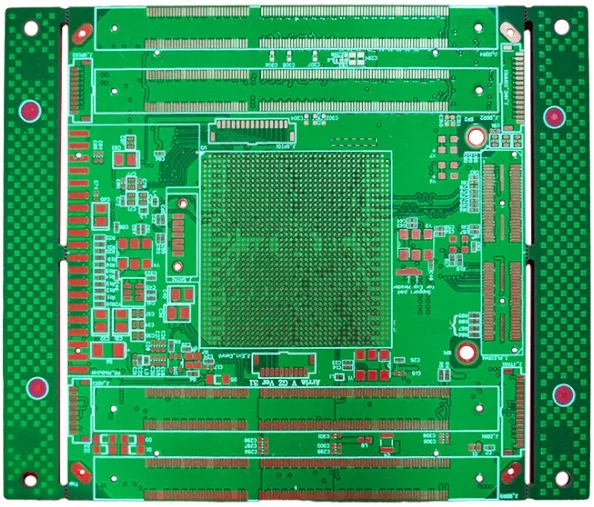
High-Density Interconnect (HDI) PCB technology represents the pinnacle of modern electronics manufacturing. As an experienced HDI PCB manufacturer, HILPCB delivers precision HDI PCB fabrication with 1+N+1 to Any-Layer ELIC build-ups, laser microvias, and VIPPO technology for compact, high-performance devices that power today's computing and communications hardware.
Understanding HDI Technology
HDI PCBs are characterized by their fine lines, small vias, and high connection pad density. These boards typically feature:
- Microvias: Holes with diameters ≤ 150μm
- Fine pitch components: BGA pitches down to 0.4mm
- Thin dielectric layers: 25-100μm thickness
- High layer counts: Up to 20+ layers in compact form factors
Manufacturing Process Overview
1. Sequential Lamination Process
The sequential build-up process is fundamental to HDI manufacturing:
Core Layer → Prepreg → Copper Foil → Lamination → Drilling → Plating
Each layer is built sequentially, allowing for precise control of impedance and signal integrity.
For the design-side decisions behind layer transitions and impedance targets, see the HDI PCB stackup design guide.
2. Micro-via Formation
Laser Drilling Technology
- CO2 lasers: For dielectric materials
- UV lasers: For copper removal
- Plasma desmear: Surface preparation for plating
Via Types in HDI
- Blind vias: Connect outer layer to inner layer
- Buried vias: Connect inner layers only
- Stacked vias: Multiple microvias in alignment
- Staggered vias: Offset microvias for routing flexibility
Advanced Quality Control
Automated Optical Inspection (AOI)
- High-resolution imaging systems
- Pattern recognition algorithms
- Defect classification and reporting
- Real-time process feedback
X-ray Inspection
- Via fill quality assessment
- Hidden defect detection
- Layer alignment verification
- Component placement validation
Electrical Testing
- In-Circuit Testing (ICT): Continuity and isolation
- Flying Probe Testing: Flexible test point access
- Boundary Scan: Digital circuit verification
Material Considerations
Substrate Materials
- Low-loss dielectrics: For high-frequency applications
- Thermally conductive materials: For heat dissipation
- Low CTE materials: Dimensional stability
Copper Foil Selection
- Ultra-thin copper: 9μm and 12μm foils
- Low-profile copper: Reduced surface roughness
- Treated copper: Enhanced adhesion properties
Design Guidelines for HDI
Via Design Rules
- Minimum via size: 100μm (4 mil)
- Via-to-via spacing: 150μm minimum
- Via-to-trace spacing: 75μm minimum
- Annular ring: 25μm minimum
Trace and Space Requirements
- Minimum trace width: 75μm (3 mil)
- Minimum spacing: 75μm (3 mil)
- Impedance tolerance: ±10%
Applications and Benefits
Consumer Electronics
- Smartphones and tablets
- Wearable devices
- Ultra-thin laptops
- Gaming consoles
Industrial Applications
- Medical devices
- Automotive electronics
- Aerospace systems
- IoT devices
Performance Advantages
- Size reduction: Up to 70% smaller than conventional PCBs
- Weight reduction: Lighter form factors
- Improved signal integrity: Shorter signal paths
- Enhanced thermal performance: Better heat dissipation
Manufacturing Challenges and Solutions
Challenge: Via Reliability
Solution: Optimized drilling parameters and advanced plating chemistry
Challenge: Layer Registration
Solution: High-precision lamination equipment with vision systems
Challenge: Yield Optimization
Solution: Statistical process control and real-time monitoring
Future Trends in HDI Technology
Emerging Technologies
- Any-layer HDI: Vias connecting any layer combination
- Embedded components: Passive components within PCB layers
- 3D printing integration: Additive manufacturing techniques
- Advanced materials: Liquid crystal polymers and ceramics
Industry 4.0 Integration
- IoT-enabled manufacturing equipment
- Predictive maintenance systems
- AI-driven quality control
- Digital twin technology
Quality Standards and Certifications
International Standards
- IPC-2226: HDI design guidelines
- IPC-6016: HDI qualification standards
- IPC-A-600: Acceptability criteria
- ISO 9001: Quality management systems
Testing Protocols
- Thermal cycling: -55°C to +125°C
- Humidity testing: 85°C/85% RH
- Mechanical stress testing
- Accelerated aging tests
Common Questions
What makes HDI PCB manufacturing different from conventional multilayer PCB production?
HDI manufacturing relies on finer traces, smaller vias, thinner dielectric layers, and sequential build-up processes that demand much tighter process control. It also uses laser drilling, advanced plating, and stricter registration management to achieve the required interconnect density.
Why are microvias so important in HDI boards?
Laser-drilled microvias reduce routing length and make it possible to connect dense fine-pitch components without consuming too much surface area. They are critical for compact layouts, but they also require precise drilling, desmear, plating, and reliability control.
Which inspections matter most for HDI quality assurance?
AOI, X-ray inspection, and electrical testing are all essential because each catches a different class of risk. AOI finds surface pattern defects, X-ray reveals hidden structural issues, and electrical tests confirm continuity and isolation across the finished board.
When should a product team choose HDI instead of a standard PCB stack-up?
HDI is usually the better choice when the design includes fine-pitch BGAs, high I/O density, strict size limits, or short high-speed interconnect requirements. If a conventional stack-up cannot route the design cleanly or would make the product too large, HDI becomes justified.
Conclusion
Advanced HDI PCB manufacturing represents a critical capability for companies seeking to develop next-generation electronic products. The combination of precision manufacturing techniques, advanced materials, and rigorous quality control enables the creation of high-performance, reliable electronic assemblies.
At HILPCB, our factory-direct HDI manufacturing lines and strict quality controls ensure that we can meet the most demanding requirements for modern electronics applications. Explore our HDI PCB capabilities or request an instant HDI PCB quote today.
For technical specifications, BGA fanout review, and custom HDI printed circuit boards, contact our DFM engineering team.