
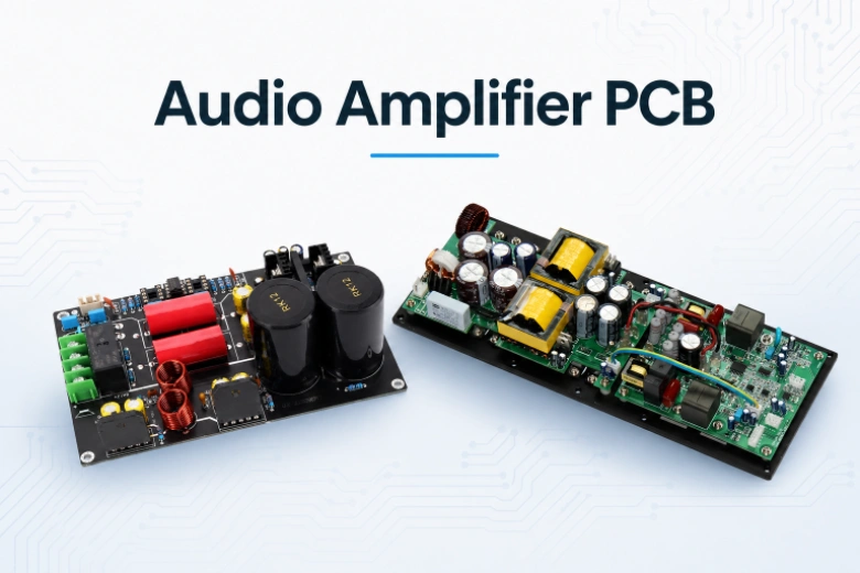
A $200 op-amp and a $2 op-amp will sound nearly identical if the PCB introduces more noise than either device generates internally. Audio amplifier layout is where the board itself becomes a component — its ground topology shapes hum rejection, its trace geometry determines channel crosstalk, and its power supply filtering decides whether you hear music or 100 kHz switching harmonics folded into the audio band. A 50 µV ground bounce between the preamp's return and the output stage's return is audible as distortion through any speaker system with 100+ dB dynamic range.
This is not a theoretical concern. The most common failure mode in audio amplifier prototypes isn't a wrong component value — it's a ground loop created by careless PCB layout, or a switching regulator whose magnetic field couples into an input trace 15 mm away. These problems don't show up in schematic simulation because simulators model ideal grounds. The PCB is where ideal meets real.
HILPCB fabricates audio amplifier boards from single-layer aluminum-core substrates for compact Class D modules through 8-layer FR-4 boards for multichannel professional amplifiers, with copper weights up to 4 oz for high-current output stages and impedance control for USB audio and RF antenna feed lines.
Menu Navigation
- Ground Topology: Where Hum Lives and Dies
- Class D Amplifier: Switching Loops and Output Filters
- Analog Power Supply Layout
- Headphone DAC and USB Audio Interface
- Tube Amplifier and High-Voltage PCB Considerations
- Thermal Design for Power Output Stages
- Manufacturing and Production Testing
Ground Topology: Where Hum Lives and Dies
Current flows in loops. When a 5 A output stage return current shares a copper path with a 50 µA preamp bias current, the voltage drop across that shared impedance modulates the preamp's reference voltage. The result — audible as hum, buzz, or distortion — cannot be removed by any downstream filter because it's already embedded in the signal.
Ground Architecture for Audio
- Hybrid Star-Plane Approach: A continuous ground plane on an internal multilayer PCB layer serves the small-signal and digital sections. The power amplifier output stage returns run separately through dedicated copper pours to the main supply ground point — typically the reservoir capacitor's negative terminal. The two ground domains connect at exactly one deliberate star point. This prevents output stage AC currents (which can be 5–10 A peak at 20 kHz) from flowing through the ground plane under the preamp input stage.
- Return Path Continuity: Every signal trace has a return current flowing in the ground plane directly beneath it. Any slot, split, or gap in the ground plane forces this return current to detour — creating a loop area that acts as both a radiating antenna and a receiving antenna for external magnetic fields. In audio, 50/60 Hz power line magnetic fields are the primary offender. A 10 cm² loop area in a preamp's return path can pick up enough 50 Hz field to produce audible hum. Rule: no interruptions in the ground plane under any signal trace, especially input traces.
- Channel-to-Channel Isolation: Left and right channels sharing a PCB must maintain >80 dB crosstalk isolation at 20 kHz. At audio frequencies, capacitive coupling between adjacent traces is the primary mechanism. Physical separation of ≥10 mm between channel traces, or dedicated ground pours between channels providing electromagnetic shielding, achieves this. For stereo PCBs, route left channel on one side of the board and right channel on the other, with a ground plane in between.
- Input Connector Grounding: RCA/XLR input ground connections tie to the ground plane at points that avoid shared impedance with the output stage. The input ground entry point should be physically close to the preamp circuit — not at the power supply end of the board where high-current return paths flow.
- Ground Lift and Safety: Balanced (XLR) audio inputs use differential signaling that rejects ground loop hum between equipment. The PCB must support both pin-1 grounded and pin-1 lifted configurations — typically a solder bridge or zero-ohm resistor option between XLR pin 1 and circuit ground.
Class D Amplifier: Switching Loops and Output Filters
Class D amplifiers switch output MOSFETs at 300 kHz–2 MHz, producing a pulse-width-modulated waveform that the output LC filter recovers as audio. Efficiency reaches 90–95%, making Class D dominant in portable speakers, soundbars, car audio, and powered studio monitors. The PCB layout challenges blend power electronics switching discipline with audio-grade noise management.
Critical Class D Layout
- Half-Bridge Switching Loop: The current loop from DC bus capacitor → high-side FET → switching node → low-side FET → capacitor return must be physically as compact as possible. Loop inductance above 1 nH generates voltage spikes during MOSFET turn-off proportional to L × di/dt. At 5 A output and 10 ns switching, even 2 nH creates a 1 V spike on a 12 V rail — enough to cause audible artifacts. Place ceramic bus capacitors (22 µF × 4 in parallel, C0G preferred for lowest ESR) directly across the FET drain-source connections, on the same PCB layer, with trace lengths under 5 mm.
- Output LC Filter Placement: The inductor (10–22 µH, ferrite or iron powder core) and film capacitor (0.47–1 µF, polypropylene) sit between the half-bridge output and the speaker terminals. The trace from the switching node to the inductor carries the full PWM waveform with sub-10 ns edges — this trace radiates EMI proportional to its length. Keep it under 10 mm. After the inductor, the signal is filtered to audio frequencies and can be routed more freely.
- Feedback Sense Point: Class D amplifiers take feedback from after the output filter. This feedback trace carries a clean audio signal and must be routed away from the switching node, the inductor (which radiates a magnetic field proportional to output current), and the gate drive traces. Route the feedback on an internal layer between ground planes for maximum shielding. Keep the feedback trace on the opposite side of the board from the power stage if possible.
- Spread-Spectrum Modulation: Modern Class D ICs (TPA3255, MA12070) use spread-spectrum clocking to distribute switching energy across a frequency band rather than concentrating it at a single frequency. This reduces peak EMI but doesn't eliminate it — the PCB layout still determines whether conducted and radiated emissions pass CISPR 32 and FCC Part 15 limits. Input and output EMI filter components placed within 10 mm of the board's power and speaker connectors.
- BTL vs. PBTL Output Configuration: Bridge-tied-load (BTL) outputs generate a differential output swing — no DC offset on the speaker. The two half-bridges' switching loops must be physically symmetrical to prevent common-mode noise on the speaker output. Asymmetric layout creates differential EMI current in the speaker cable, which radiates. Parallel bridge-tied-load (PBTL) doubles output current — requiring wider traces and heavier copper on heavy copper PCBs.
Analog Power Supply Layout
The power supply determines headroom, dynamic capability, and noise floor. Whether using a linear supply or SMPS, the PCB layout of the power section requires as much attention as the signal path — more, actually, because power supply noise affects every stage simultaneously.
Power Supply PCB Engineering
- Linear Supply Routing: Rectifier diodes conduct in short, high-current pulses at twice the mains frequency. The loop from transformer secondary → bridge rectifier → first reservoir capacitor must be compact, with heavy copper traces (2 oz minimum) to reduce resistance. The reservoir capacitor placement defines the grounding reference for the entire amplifier — this is the star point in a star ground scheme. Long traces between rectifier and reservoir add impedance that appears as supply sag during bass transients.
- SMPS Section Isolation: Switch-mode power supplies generate noise at 100–500 kHz and harmonics. On the PCB, the SMPS section must be physically isolated from the analog signal path — separated by at least 20 mm of continuous ground plane with no signal traces crossing the boundary. The SMPS inductor's magnetic fringing field extends 5–10 mm in all directions — no sensitive analog traces within that zone. Input and output filter capacitors (low-ESR X7R or X5R ceramics) placed within 5 mm of the switcher IC.
- Per-Stage LDO Post-Regulation: Each analog gain stage benefits from its own dedicated LDO regulator fed from the main supply rail. A 100 nF ceramic + 10 µF electrolytic/polymer on each supply pin, placed within 5 mm of the IC. For ultra-low-noise preamp stages (phono preamps, microphone preamps), an additional RC or LC filter network on the supply rail creates a quiet "island" power domain. Target: <10 µVrms supply ripple for phono stages, <100 µVrms for line-level stages.
- Bipolar Supply Symmetry: Audio amplifiers using ±15 V or ±30 V bipolar supplies require symmetric trace impedance between +V and -V rails. Asymmetric voltage drop under dynamic load generates even-harmonic distortion — audible as a harsh coloration. Route positive and negative supply traces as closely-spaced pairs on adjacent layers or as parallel traces on the same layer.
- Bulk Capacitor Selection: Electrolytic reservoir capacitors dominate the power supply's transient response. ESR at 20 kHz (not DC ESR) determines how much voltage sag occurs during bass transients. Multiple smaller capacitors in parallel achieve lower total ESR than a single large capacitor — four 2,200 µF in parallel beats one 10,000 µF. PCB pad geometry must accommodate the chosen capacitor form factor with adequate pin spacing for soldering reliability.
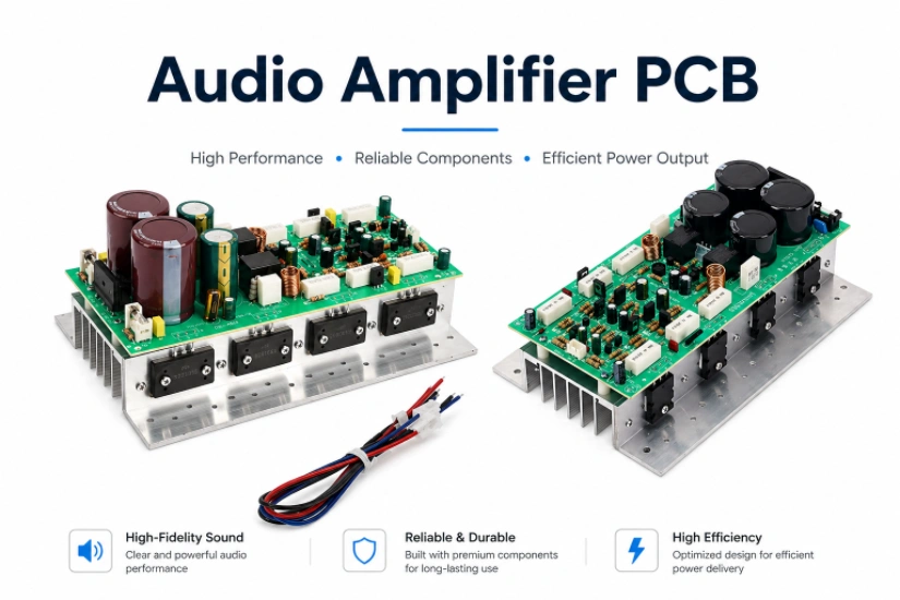
Headphone DAC and USB Audio Interface
Desktop headphone amplifiers and USB DACs combine a USB interface (USB Audio Class 2.0), a DAC chip (ESS ES9038Q2M, AKM AK4499, Cirrus Logic CS43131), analog output filtering, and a headphone driver on a single board. These designs represent the highest signal-to-noise ratio achievable on a consumer PCB — 120+ dB SNR requires layout discipline that approaches instrumentation-grade design.
Digital-Analog Partitioning
- Physical Board Partition: Digital components (USB PHY, XMOS processor, clock generator, I²S data lines) on one board section; analog components (DAC current output, I/V conversion stage, low-pass filter, headphone amplifier) on the other section. The two domains connect only through the DAC chip itself and its power supply filtering. No other traces cross the boundary — no ground plane stitching between domains except at the DAC's own ground connection. This forces all digital return currents to flow back through the DAC's ground pins rather than through the analog ground plane.
- Master Clock Jitter Control: The DAC's master clock (typically 22.5792 MHz or 24.576 MHz, or both for 44.1/48 kHz family sample rates) directly determines conversion accuracy. Clock jitter of 1 ps RMS degrades THD+N by approximately 6 dB at 20 kHz on a 120 dB SNR DAC. The clock oscillator sits within 10 mm of the DAC's clock input pin, with a short trace over continuous ground plane. No vias in the clock trace if possible — each via adds approximately 30 pH of inductance that creates impedance discontinuity at the clock's harmonic frequencies.
- USB Interface Layout: USB 2.0 differential pair at 90 Ω ±10% impedance, routed on high-speed PCBs with TDR-verified impedance control. ESD protection (TVS diodes) within 5 mm of the USB-C connector pads. Connector shell connected to chassis ground through a separate path from signal ground — preventing USB host computer noise from entering the audio ground reference through the shield connection.
- I²S Bus Routing: I²S signals (BCLK, LRCLK, DATA, MCLK) between the USB processor and DAC run at 3–50 MHz depending on sample rate and bit depth. These are digital signals that radiate — route on internal layers sandwiched between ground planes. Keep I²S traces >10 mm from any analog signal trace. Series termination resistors (33–47 Ω) at the driver output pins suppress overshoot that would otherwise radiate.
- Headphone Output Stage: Headphone amplifiers drive loads from 16 Ω to 600 Ω — a 37.5:1 impedance range. The output coupling capacitors (if used in AC-coupled designs) must be low-ESR types (polymer or film) to avoid bass rolloff into low-impedance loads. PCB trace resistance from the amplifier output to the headphone jack should be <50 mΩ to avoid damping factor degradation — use 2 oz copper or wide traces (≥40 mil).
Tube Amplifier and High-Voltage PCB Considerations
Vacuum tube (valve) amplifiers present unique PCB challenges that differ fundamentally from solid-state design. High voltages (250–500 V B+), high-impedance circuit nodes susceptible to stray capacitance pickup, microphonic sensitivity, and component values that haven't changed since 1960 require layout practices borrowed from neither digital nor standard analog PCB design.
Tube Amp PCB Layout
- High-Voltage Clearance: B+ supply traces carrying 300–500 V DC require creepage and clearance distances per IPC-2221. On uncoated external layers at Pollution Degree 2, 500 V requires approximately 2.5 mm clearance. With conformal coating, reduced distances may be acceptable — but the coating must be verified to cover all high-voltage gaps. Some designers route high-voltage and low-voltage sections on opposite sides of the board with no through-hole connections between them, using transformer coupling for the interface.
- Tube Socket Pin Routing: Noval (9-pin) and octal (8-pin) tube sockets have pins arranged on a circle. The grid input trace and the plate output trace must not run parallel — this creates Miller capacitance feedback paths that can cause oscillation. Route the grid input to one side and the plate output to the opposite side, with ground copper between them. This replicates the classic point-to-point wiring topology in PCB form.
- Heater Wiring: Tube heaters draw 0.3–1.6 A at 6.3 V or 12.6 V AC/DC. The heater traces must be heavy enough (≥30 mil at 1 oz copper for 1 A) to avoid voltage drop that shifts tube operating points. Route heater traces as adjacent differential pairs to cancel the magnetic field that would otherwise induce 50/60 Hz hum into nearby high-impedance grid circuits. Elevate the heater DC bias to a positive voltage (typically +30–50 V) to reduce cathode-heater leakage current that causes hum.
- Coupling Capacitor Placement: Inter-stage coupling capacitors (typically 0.022–0.47 µF film) carry the full audio signal at high impedance. These components are physically large and their leads are sensitive to vibration-induced microphonics. Mount coupling capacitors flat to the board and secure with adhesive in vibration-prone applications (guitar amplifiers, live sound equipment).
Thermal Design for Power Output Stages
A 100 W per channel Class AB amplifier dissipates 60–100 W as heat at typical listening levels (Class AB efficiency is 25–60% depending on signal level). Even high-efficiency Class D designs dissipate 5–15 W per channel at full power in thermally-limited packages.
Board-Level Thermal Management
- Output Transistor Mounting: TO-247 or TO-264 output devices mount to external heatsinks through the PCB using thermal pad connections. The PCB traces connecting collector/drain to the circuit carry the full output current — use heavy copper (2–3 oz) for these traces. Thermal relief pads on mounting holes allow heat to conduct through the bolt into the heatsink without excessive lateral heat transfer into the FR-4 that could cause warpage.
- Class D Thermal Pad Design: Integrated Class D ICs (TPA3255, MA12070P) dissipate heat through an exposed thermal pad on the package bottom. Thermal via arrays (0.3 mm drill, 0.8 mm pitch, covering ≥70% of the thermal pad area) transfer heat to the opposite board surface where it conducts into a heatsink or copper pour. HILPCB's via-in-pad filling process ensures reliable solder joint formation over the via array.
- Component Placement for Thermal Management: Temperature-sensitive components — voltage references, bias setting resistors, input stage transistors — placed upstream in the natural convection airflow path (below the heatsink in a vertical orientation, or before the heatsink in a horizontal forced-air configuration). Power supply rectifiers and voltage regulators placed near the heatsink where temperature rise is acceptable.
- Copper Pour Heat Spreading: Large copper pours on both board surfaces, connected through thermal via arrays, spread heat from localized hot spots. A 1 oz copper pour has thermal conductivity of 390 W/m·K — 1,000× better than the FR-4 substrate it covers. For amplifiers without external heatsinks (Bluetooth speakers, soundbars), the PCB's copper is the primary thermal path.
Manufacturing and Production Testing
Audio-Specific Production
- Prototype Assembly: 5–20 boards for listening evaluation, THD+N measurement, and EMC pre-compliance testing. Mixed SMT/through-hole for boards combining SMD ICs with through-hole connectors, potentiometers, and output transistors. 5–7 day turnaround.
- SMT Assembly: Automated placement for 0201 decoupling capacitors, QFN/QFP audio ICs, and fine-pitch USB-C connectors. Reflow profiling optimized for boards with both ceramic and electrolytic capacitors — avoiding thermal damage to polymer caps while achieving complete solder wetting on thermal pads.
- Volume Production: Panel optimization for guitar amp boards (often irregular shapes with large cutouts), functional test fixture development for automated audio output verification, and consistent solder paste deposition for repeatable channel matching across production lots. 500–50,000 units/year.
- Impedance Control: USB differential pairs at 90 Ω, I²S clock traces, and Bluetooth/Wi-Fi antenna feed lines require controlled impedance fabrication with TDR verification. Most analog audio traces do not require impedance control, but consistent trace width and ground plane spacing maintain predictable parasitic behavior.
Discuss your audio amplifier PCB project with our analog-experienced engineering team →
Frequently Asked Questions
Why is ground topology so critical in audio amplifier PCBs? In an audio PCB, current flowing through shared ground traces creates small voltage drops. If a high-current output return shares a ground path with a sensitive preamp input, that voltage drop modulates the input signal, creating audible hum or distortion. A proper "hybrid star-plane" grounding scheme physically separates power returns from small-signal grounds to prevent this.
How does a PCB layout affect a Class D amplifier's noise? Class D amplifiers switch at high frequencies (300 kHz–2 MHz). The PCB trace loop connecting the DC capacitors, MOSFETs, and ground (the half-bridge switching loop) must be extremely short. If this loop has parasitic inductance, it generates massive voltage spikes that cause audible artifacts and severe electromagnetic interference (EMI).
Why do high-end audio DACs require physically partitioned boards? A DAC converts noisy digital data into pristine analog audio. To achieve a 120+ dB Signal-to-Noise Ratio (SNR), the PCB must be physically partitioned. Digital components (like USB interfaces) sit on one side, and analog components sit on the other. Ground planes must never overlap, forcing digital return currents to stay completely isolated from the sensitive analog output.
What are the thermal challenges of power output stages on a PCB? Audio amplifiers can dissipate 60–100W of heat at typical listening levels. For board-mounted components, the PCB must act as a thermal spreader. This requires using heavy copper (2–3 oz) to conduct heat away from the components, and dense thermal via arrays beneath the ICs to transfer heat straight through the board into an external heatsink.