
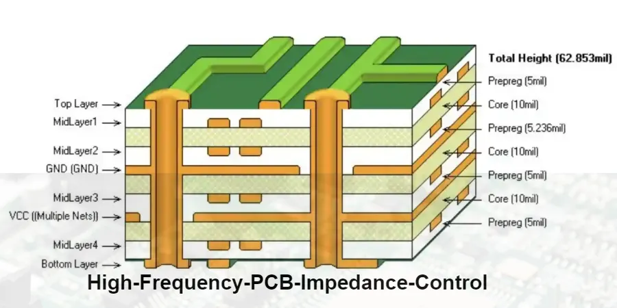
Choose backdrilling based on the signal bandwidth, via stub length, stack-up geometry, and supplier process capability—not only the data rate. A production-ready decision requires the maximum remaining stub length, backdrill diameter, stop layer, depth tolerance, impedance target, stack-up drawing, and verification evidence from the PCB manufacturer. For high-speed designs above 10–25 Gbps, unused via stubs can create reflections and insertion loss problems. The correct decision is whether controlled-depth drilling, HDI vias, or standard through vias provide the best balance of signal integrity, manufacturing risk, and cost.
What technical data should be confirmed before selecting backdrill?
A backdrill request should start with four engineering inputs:
| Decision parameter | Values to define | Evidence required |
|---|---|---|
| Signal integrity target | PCIe 3.0 at 10 Gbps, PCIe 4.0/5.0, 25 Gbps, 56 Gbps PAM4, 112 Gbps PAM4, HDMI or USB differential requirements | Channel simulation, impedance report, loss budget |
| Impedance requirements | Single-ended 50 Ω, differential 90 Ω/100 Ω, tolerance such as ±7% | Stack-up impedance calculation and TDR coupon results |
| Via stub limit | Target remaining stub typically <10 mil (254 µm) for demanding high-speed channels; source design examples include <8 mil targets | Microsection or cross-section verification |
| Manufacturing capability | Backdrill depth control, drill diameter, copper clearance, stop-layer accuracy | Fabricator DFM review and capability statement |
The key calculation is the relationship between rise time and stub length. A common engineering guideline is:
Stub length (inches) < 0.15 × Trise / Tpd
For 28 Gbps NRZ designs, remaining stub length is commonly controlled within approximately 10 mil (254 µm).
Which PCB manufacturers provide backdrill planning data?
Several PCB manufacturers publish independent guidance. Their published data shows where engineers usually need additional supplier confirmation:
| Manufacturer page | Technical data provided | Remaining decision gap |
|---|---|---|
| Typical fabricator backdrill application notes | Explain via stub removal, larger re-drill tools, layer transition examples, signal integrity impact, deterministic jitter and BER effects, stub resonance, remaining stub ranges of 0.1–0.25 mm, stop-layer concepts, and drawing requirements | Rarely ship a complete RFQ package defining every fabrication file, supplier acceptance criteria, and stack-up decision path; procurement teams still need measurable evidence such as cross-sections and capability verification |
| APTPCB backdrill planning guide | Provides target stub length of 10 mil (0.25 mm) or less, drill oversize of 8–10 mil (0.2–0.25 mm), depth tolerance of ±5 mil (±0.125 mm), clearance guidance, layer planning steps, and inspection recommendations | Engineers still need to match these limits to their exact stack-up dielectric thickness and channel requirements |
The supplier selection decision should not be based only on whether a PCB factory advertises backdrilling. The important question is whether the manufacturer can translate your released design data into controlled drilling results and provide verification.
When does a PCB design need backdrilling instead of standard vias?
Backdrilling becomes increasingly valuable when unused plated-through-hole barrel sections become electrically significant.
Use backdrilling when:
- Data rates exceed approximately 10–25 Gbps and via stubs affect channel performance.
- Thick multilayer boards create long unused via sections.
- High-speed SerDes, backplanes, line cards, PCIe, DDR interfaces, or other critical channels require reduced reflection.
- Blind/buried vias are not economically practical.
A typical example:
A signal routes from L1 to L3 on a 12-layer PCB. A standard through via continues from L1 to L12, leaving the L4–L12 copper barrel unused. Backdrilling from L12 toward L3 removes the unwanted stub.
A fabrication note can specify:
Backdrill: L12 to L3, Target Remaining Stub <8 mil
What backdrill parameters should be included in a PCB fabrication drawing?
A complete backdrill specification should include:
- Backdrill side: top, bottom, or both.
- Start layer and stop layer.
- Finished backdrill diameter.
- Original via diameter.
- Maximum remaining stub length.
- Drill depth tolerance.
- Copper clearance requirements.
- Separate NC drill files for each backdrill depth.
- “Must Not Cut” layers.
Typical values:
| Parameter | Typical engineering value | Risk if not defined | Verification |
|---|---|---|---|
| Backdrill diameter increase | 8–10 mil (0.2–0.25 mm) larger than original via | Residual barrel copper remains | Drill drawing review and cross-section |
| Remaining stub target | <10 mil (254 µm); some designs specify <8 mil | Reflection and insertion loss | Microsection measurement |
| Depth control | ±50 µm (2 mil) capability from source manufacturing specification; other suppliers publish ±5 mil (±0.125 mm) | Excessive removal or remaining stub | Supplier capability report |
| Signal threshold example | >10 Gbps critical nets | High-speed degradation | SI simulation |
How should engineers calculate maximum allowable stub length by data rate?
The Bogatin rule provides a quick first-pass estimate for the maximum allowable via stub length before channel simulation: max stub (inches) = 0.3 ÷ Gbps. The table below applies this rule across common data rates and pairs it with practical residual stub targets, drill oversize guidance, and the relative manufacturing challenge.
| Data rate | Max stub per Bogatin rule | Max stub in mm | Recommended residual stub target | Drill oversize | Manufacturing challenge |
|---|---|---|---|---|---|
| 5 Gbps | 60 mil | 1.5 mm | <15 mil | 8–10 mil standard | Easy |
| 10 Gbps | 30 mil | 0.76 mm | <10 mil | 8–10 mil | Easy |
| 16 Gbps | 19 mil | 0.48 mm | <8 mil | 6–8 mil | Moderate |
| 25 Gbps | 12 mil | 0.30 mm | <5 mil | 6–8 mil | Moderate |
| 32 Gbps | 9 mil | 0.23 mm | <4 mil | 4–6 mil | Difficult |
| 56 Gbps | 5 mil | 0.13 mm | <3 mil | 4–6 mil | Very difficult |
| 112 Gbps | 2.5 mil | 0.06 mm | <2 mil | 3–5 mil | Extreme |
The Bogatin rule gives a theoretical upper bound. Production designs should target a residual stub well below the calculated maximum—typically 50% or less—to account for stack-up tolerance, drill depth variation, and impedance discontinuity at the stub tip. At 56 Gbps and above, the required residual stub approaches the limit of mechanical drilling capability, and engineers should evaluate blind-via or HDI alternatives alongside backdrilling.
How should materials and stack-up choices affect backdrill planning?
Backdrill performance depends on the complete transmission path. Material selection controls dielectric behavior, loss, thermal reliability, and impedance geometry.
| Material class | Example materials | Dk @10 GHz | Df @10 GHz | Tg °C | Td °C | CTI | Decision impact |
|---|---|---|---|---|---|---|---|
| Standard FR-4 | S1141, KB-6160 | ~4.2 | ~0.020 | 140 | 315 | 175 | Cost-focused designs with lower bandwidth requirements |
| Mid-loss/high-Tg | IT-180A, S1000-2M | ~3.8 | ~0.012 | 180 | 345 | 175 | Servers, industrial control, DDR4 |
| Low loss | IT-968, M4S | ~3.6 | ~0.007 | 190 | 360 | 600 | PCIe 4.0/5.0 and 25 Gbps backplanes |
| Very low loss | Megtron 6, IT-988GSE | ~3.2 | ~0.003 | 210 | 400 | 600 | 56/112G PAM4 |
| RF/microwave | Rogers RO4350B | 3.48 | 0.0037 | 280 | 390 | 175 | mmWave radar and 5G antenna applications |
| Flexible polyimide | Dupont AP, Shengyi SF305 | ~3.4 | ~0.002 | >300 | >500 | - | Flex-rigid applications |
For example, a 100 Ω differential pair with a 4 mil dielectric thickness may require approximately:
- IT-180A (Dk ~3.8): ~4.5 mil trace width.
- Megtron 6 (Dk ~3.2): ~5.2 mil trace width.
Lower Dk can allow wider traces, reducing conductor loss and improving manufacturing tolerance, but premium materials create a higher material cost tradeoff.
Which PCB stack-up structures support reliable high-speed routing?
| Layer count | Example structure | Engineering decision |
|---|---|---|
| 4-layer | S1 / G2 / P3 / S4 | Lowest cost option for IoT and MCU designs |
| 6-layer | S1 / G2 / S3 / S4 / P5 / S6 | Common high-speed structure with inner stripline routing |
| 8-layer | S1 / G2 / S3 / P4 / G5 / S6 / P7 / S8 | Provides two controlled stripline regions and stronger plane coupling |
| 10-layer | S1 / G2 / S3 / P4 / G5 / S6 / G7 / P8 / S9 / S10 | Better separation for high-speed digital and sensitive circuits |
High-speed signals should maintain a continuous reference plane. Critical nets should avoid crossing plane splits. Inner-layer stripline routing generally provides stronger EMI control than outer-layer microstrip routing.
How do copper weight and thermal requirements change the PCB decision?
Copper thickness affects routing density, power delivery, and manufacturability.
Typical copper choices:
- Signal layers: 0.5 oz (18 µm) or 1 oz (35 µm).
- Power/ground planes: 1 oz standard.
- High-current regions: consider 2 oz (70 µm) or thicker.
- Above 50 A total board current or localized high-current paths, heavier copper may be required.
A 2 oz copper design can make fine routing more difficult. Achieving less than 4 mil trace/space becomes challenging because thicker copper reduces etching precision.
Thermal reliability decisions should also consider dielectric thermal conductivity. Typical dielectric ranges are approximately:
- Standard dielectric: 1.5–3 W/mK.
- High-performance thermal materials: 4–8 W/mK.
For thermal management applications, MCPCB structures using aluminum or copper bases can transfer heat more effectively than standard FR-4.
What manufacturing evidence should engineers request after fabrication?
The released board should be verified through:
- Impedance coupon testing using TDR.
- Microsection analysis of backdrilled vias.
- Stack-up verification.
- Copper thickness verification.
- Thermal test reports when thermal performance is a design requirement.
A production stack-up document should include:
- Layer construction.
- Core and prepreg thickness.
- Copper thickness.
- Final pressed thickness.
- Material model.
- Controlled impedance geometry.
- Backdrill depth and stop layer.
What files and specifications should be included in a PCB RFQ?
Submit these files and requirements to the PCB supplier:
Design files
- Gerber fabrication files.
- Drill files including separate backdrill NC drill files.
- PCB stack-up drawing.
- BOM.
- Pick-and-place files if assembly is included.
- Via drawing.
- Fabrication drawing with backdrill annotations.
- Impedance requirements.
- Material requirements.
Supplier evidence to request
- DFM review of the stack-up and backdrill plan.
- Backdrill capability specification.
- Cross-section or microsection report.
- TDR impedance report.
- Material datasheets.
- Thermal test report when thermal performance is required.
- Final inspection documentation.
How does HILPCB support backdrill and stack-up decisions?
HILPCB provides stack-up engineering support for designs requiring controlled impedance, high-speed materials, and specialized PCB structures.
Capabilities from the source design include:
- Maximum layer count: 64 layers.
- Minimum trace/space: 2.5 / 2.5 mil.
- Backdrill depth control: ±50 µm (2 mil).
- Supported materials: FR-4, Rogers, Taconic, Arlon, Isola, Nelco, Shengyi, Panasonic Megtron, and other material families.
- Processes: HDI (any-order), flex-rigid, embedded resistors/capacitors, heavy copper, and ceramic substrates.
Related solutions:
- PCB Fabrication
- HDI PCB
- PCB Assembly
- Flex-rigid PCB
Conclusion: What is the final backdrill planning decision?
A reliable backdrill plan connects electrical requirements with manufacturing evidence. Define the signal bandwidth, calculate allowable stub length, select the stack-up and material system, specify backdrill geometry, and require verification through cross-section and impedance testing. The correct choice is not always maximum backdrilling—it is the smallest manufacturing change that meets the channel performance target.
Which deliverable would help next: RFQ checklist or stack-up template?