
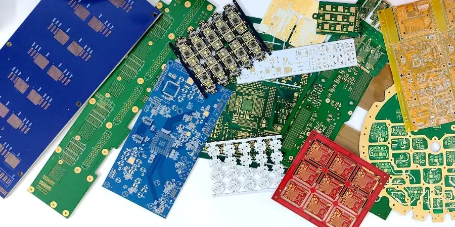
Reference images illustrate PCB structure and layout; they are not biodegradability test evidence.
Electronics waste is a major environmental concern. Research into cellulose-, paper- and biopolymer-based substrates may help reduce persistent substrate waste in selected short-life applications. However, a board with a degradable substrate is not necessarily a biodegradable electronic assembly: copper, solder, coatings, components and recycling processes must also be considered.
For a HILPCB feasibility discussion, separate conventional requirements such as halogen-free laminate or lead-free assembly from an experimental biodegradable substrate. Confirm material availability, processing and qualification evidence before treating a research concept as a commercial manufacturing option. Environmental benefit also requires a defined life-cycle and end-of-life comparison.
What is a Biodegradable PCB?
A biodegradable-substrate PCB uses a material engineered to break down under defined conditions; biodegradation must be demonstrated using a specified test method and environment. Lead-free solder is not itself biodegradable, and conventional FR-4, copper traces and electronic components do not disappear when a board is composted.
The key components of a Biodegradable PCB include:
- Candidate substrates: Research materials include cellulose, paper and selected biopolymers, with moisture and service-life limitations that must be qualified.
- Assembly materials: Lead-free solder can reduce intentional lead use but does not make the assembly biodegradable; assess metals, residues and disassembly.
- Sustainable design: Minimizing the use of hazardous chemicals in manufacturing while ensuring the PCB retains its functionality for a reasonable lifespan.
Such approaches may suit carefully qualified disposable sensors and experimental devices; they are not drop-in replacements for long-life, safety-critical or high-temperature FR-4 products.
Why Biodegradable PCBs Matter
Conventional FR-4 is a persistent thermoset composite and does not become compostable because an assembly uses lead-free solder. A degradable substrate may reduce one part of the persistent waste stream, but the result depends on material composition, use conditions and the treatment of the remaining assembly. Decomposition time depends on the material, exposure conditions and measured endpoint.
Document what degrades, what remains and where each fraction goes. Substrate disintegration is not proof that the metals, components or additives have biodegraded or that the complete assembly is suitable for an ordinary compost stream.
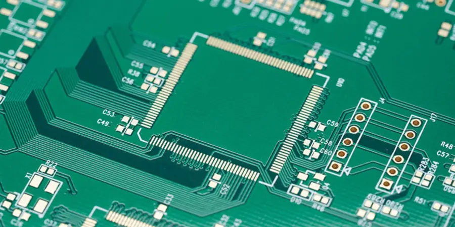
Applications of Biodegradable PCBs
Research into biodegradable substrates includes printed sensors and flexible-electronics demonstrators. Application suitability must be established for a particular construction; smartphones, computers and long-life wearables are not automatically good candidates merely because they contain electronics.
| Candidate use | Service requirements to verify | End-of-life question |
|---|---|---|
| Short-life sensor or tag | Moisture, temperature, handling, measurement stability and intended life | Can conductors and components be recovered after the substrate's defined treatment? |
| Flexible wearable demonstrator | Sweat/humidity, bending, skin-contact and electrical safety requirements | Which materials remain, and how will the used device be collected? |
| Packaging electronics | Printing/assembly compatibility, storage and product handling | Does the electronic section have a collection/recovery route compatible with the packaging? |
| Medical research device | Application-specific safety, biocompatibility and sterilization evidence | What controlled treatment is required for used materials? Biodegradability alone does not establish implant suitability |
What Evidence Does a Biodegradable Substrate Need?
Evaluate the material through two separate gates: it must work for its intended service life, and the claimed end-of-life behavior must be demonstrated under stated conditions.
- Material identity: Exact composition, fillers, adhesives, conductors and any protective layers; paper or a biopolymer family name is not a qualification.
- Electrical and assembly behavior: Conductor adhesion, resistance/insulation, moisture response, mechanical strength and compatibility with the actual printing or attachment process.
- Degradation evidence: Test method, environment, time, sample construction and measured endpoint. Distinguish biological degradation from fragmentation or dissolution.
- Recovery and impact: Identify remaining metals/components, collection and treatment steps. Compare environmental impacts at a stated life-cycle boundary rather than assuming a renewable feedstock proves a lower total impact.
Manufacturing Review with HILPCB
HILPCB is investing in biodegradable-PCB research and development and collaborating with suppliers on material and process development. HILPCB offers rapid PCB prototyping, flexible low- and volume-quantity production, and collaborative custom design, material-selection and quality support for standard and available constructions. These ordinary services do not establish that an experimental biodegradable substrate is commercially available or qualified; evaluate that material and process separately.
A conventional high-Tg PCB is not a biodegradable alternative. For a proposed research substrate, provide its supplier data, samples, conductor/attachment process, service environment and acceptance criteria. Confirm whether the requested fabrication or assembly process is available and compatible before ordering; no generic biodegradable-PCB production capability should be inferred from standard FR-4 services.
A Gerber Viewer and impedance calculator can support design review. They do not establish material durability, biodegradation, compostability or a life-cycle benefit. Use manufactured samples and suitable tests for those claims.
| RFQ or research input | Evidence to request before release |
|---|---|
| Material and conductor stack | Identified grades, process limits and approved substitutions |
| Assembly plan | Component attachment, thermal exposure, cleaning and inspection compatibility |
| Functional/service life | Defined electrical, moisture, mechanical and storage tests |
| Environmental claim | Degradation report covering the stated material/sample and environment |
| End-of-life plan | Remaining-material identification and feasible recovery/treatment route |
| Quantity and schedule | Build-specific feasibility, sample plan and quotation |
State the approved service and end-of-life claims separately. A successful laboratory demonstrator does not establish production readiness or unchanged performance across other applications.
Is there a "pcb green" or eco friendly PCB option?
"Green PCB" may mean lead-free solder, halogen-free laminates or potentially lower-impact manufacturing practices. These are not synonyms for biodegradable or compostable PCBAs; evaluate claims against measured environmental performance and relevant end-of-life regulations.