
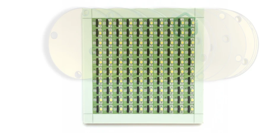
Ceramic PCB manufacturing is designed for electronic systems that require high thermal conductivity, electrical insulation, dimensional stability, and long-term reliability. Unlike conventional FR-4 circuit boards, ceramic substrates can withstand higher temperatures, dissipate heat more efficiently, and maintain stable performance in demanding operating environments.
HILPCB manufactures ceramic PCBs using advanced technologies including Direct Bonded Copper (DBC), Direct Plated Copper (DPC), and High-Temperature Co-Fired Ceramic (HTCC). These manufacturing methods support applications such as power semiconductor modules, RF systems, LED packages, automotive electronics, aerospace equipment, and industrial control systems.
The Core Advantages of Ceramic PCB Materials
Ceramic PCB materials combine high thermal performance with excellent electrical insulation. Common ceramic substrate materials include Aluminum Oxide (Al₂O₃), Aluminum Nitride (AlN), and Silicon Nitride (Si₃N₄). Each material provides different performance characteristics for thermal management, mechanical strength, and electrical requirements.
Compared with organic PCB materials, ceramic substrates provide better stability under high temperature cycling, high voltage operation, and harsh environmental conditions.
Key Benefits Include:
- High Thermal Conductivity: Ceramic substrates efficiently transfer heat away from power components. Thermal conductivity ranges from approximately 24 W/m·K for standard Al₂O₃ ceramics to more than 180 W/m·K for advanced AlN materials, helping maintain component temperature control and improve system reliability.
- Excellent Electrical Insulation: Ceramic materials provide high dielectric strength and insulation resistance, making them suitable for high-voltage power circuits and semiconductor packaging.
- Low Coefficient of Thermal Expansion (CTE): Ceramic CTE values are close to semiconductor materials such as silicon, reducing mechanical stress caused by repeated thermal expansion and contraction.
- Strong Environmental Resistance: Ceramic substrates resist corrosion, moisture, chemical exposure, and oxidation, supporting operation in industrial and medical environments.
- Long-Term Mechanical Reliability: The rigid ceramic structure provides stable performance under vibration, thermal shock, and demanding operating conditions.
These properties make ceramic PCBs suitable for mission-critical systems where heat management and reliability are more important than the low cost of standard PCB materials.
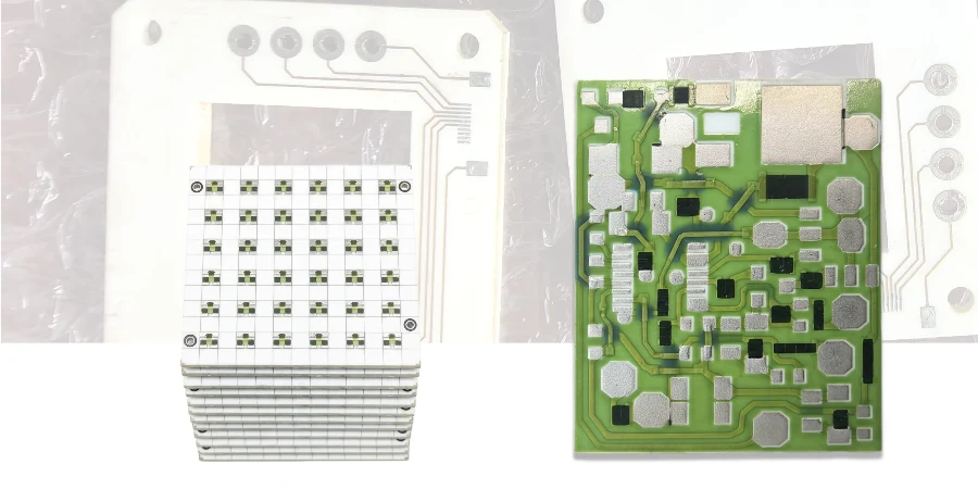
A Deep Dive into Core Manufacturing Technologies: DBC, DPC, & HTCC
Ceramic PCB manufacturing uses different processes depending on electrical performance, thermal requirements, circuit density, and operating environment. The three major technologies used in ceramic circuit production are Direct Bonded Copper (DBC), Direct Plated Copper (DPC), and High-Temperature Co-Fired Ceramic (HTCC).
Each process provides different advantages for power electronics, precision circuits, and high-temperature applications.
1. Direct Bonded Copper (DBC)
Direct Bonded Copper (DBC) technology bonds copper foil directly onto a ceramic substrate using a high-temperature eutectic bonding process. The bonding process typically occurs above 1000°C and creates a strong Cu-O eutectic connection between copper and ceramic without using an adhesive layer.
DBC commonly uses Aluminum Oxide (Al₂O₃) or Aluminum Nitride (AlN) ceramic substrates combined with thick copper layers for high-current applications.
Core Advantages:
- High Bond Strength: The direct copper-to-ceramic bond provides strong mechanical reliability and resistance to thermal shock.
- High Current Capability: Copper thickness typically ranges from 127µm to more than 300µm, allowing DBC substrates to support high-current power applications.
- Excellent Thermal Cycling Performance: The compatible thermal expansion characteristics of copper and ceramic improve reliability during repeated temperature changes.
Ideal Applications:
DBC is widely used in power semiconductor applications including IGBT modules, MOSFET power devices, electric vehicle inverters, renewable energy converters, industrial motor drives, and high-power switching systems.
2. Direct Plated Copper (DPC)
Direct Plated Copper (DPC) is a thin-film ceramic PCB manufacturing process that creates high-precision copper patterns directly on ceramic substrates. The process starts with sputtering a thin copper seed layer onto the ceramic surface. Photolithography defines the circuit pattern, followed by electroplating to increase copper thickness.
DPC is optimized for applications requiring fine traces, high-density interconnects, and precise circuit geometries.
Core Advantages:
- High Circuit Precision: DPC supports fine line and space designs down to 20µm with excellent pattern definition.
- Three-Dimensional Interconnect Capability: The process supports plated vias and vertical connections for advanced packaging structures.
- Excellent Surface Flatness: Thin-film processing provides a smooth surface suitable for precision components and semiconductor packaging.
Ideal Applications:
DPC is commonly used in RF and microwave circuits, high-density sensors, chip-on-board LED packages, and Thin Film PCB applications where circuit accuracy and miniaturization are critical.
3. High-Temperature Co-Fired Ceramic (HTCC)
High-Temperature Co-Fired Ceramic (HTCC) uses multiple layers of ceramic green tape combined with printed conductive materials such as tungsten and molybdenum. The stacked layers are fired together at temperatures exceeding 1600°C, creating a dense ceramic structure with integrated electrical pathways.
HTCC technology enables multilayer ceramic circuits that maintain performance in extreme environments.
Core Advantages:
- High Mechanical Strength: The fully sintered ceramic structure provides excellent resistance to vibration, shock, and mechanical stress.
- Hermetic Protection: The dense ceramic body provides natural hermetic sealing, protecting internal circuits from moisture and contaminants.
- High Temperature Operation: HTCC circuits can operate continuously at temperatures of 500°C and beyond, depending on design and materials.
Ideal Applications:
HTCC is used in aerospace electronics, automotive engine control systems, downhole drilling equipment, and implantable medical devices where reliability under extreme conditions is required. For more details, see our guide on HTCC PCB technology.
| Feature | Direct Bonded Copper (DBC) | Direct Plated Copper (DPC) | High-Temp Co-Fired Ceramic (HTCC) |
|---|---|---|---|
| Core Process | High-Temperature Eutectic Bonding | Sputtering + Electroplating | Multilayer Co-Firing |
| Conductor | Pure Copper (Cu) | Pure Copper (Cu) | Tungsten (W), Molybdenum (Mo) |
| Key Advantage | High Current, High Reliability | High Precision, High Density | Robust, Hermetic, High Temp |
| Primary Application | Power Electronics | RF, LED, Sensors | Aerospace, Harsh Environments |
Surface Preparation and Metallization
The metallization process determines the electrical reliability and mechanical strength of ceramic PCBs. Ceramic surfaces require careful preparation because the material has low surface roughness and does not naturally bond with metals.
Before copper or conductive materials are applied, each ceramic substrate undergoes surface treatment to improve adhesion and ensure consistent metallization quality.
At HILPCB, ceramic substrate preparation may include ultrasonic cleaning, chemical degreasing, and plasma activation. These processes remove contaminants and improve surface wettability for uniform metal deposition.
Common metallization methods include:
- Sputtering (PVD) or Evaporation: Used for DPC and thin-film ceramic circuits requiring fine patterns and precise conductive layers.
- Screen-Printed Thick Film Pastes: Used for HTCC and hybrid ceramic circuits with materials such as silver, gold, tungsten, or molybdenum.
- Electroplating and Electroless Copper Deposition: Used to increase copper thickness for high-current conductors and multilayer interconnections.
After metallization, ceramic PCBs can receive surface finishes including ENIG, ENEPIG, immersion silver, hard gold, or plated nickel-gold. These finishes improve solderability, oxidation resistance, and wire bonding performance during Ceramic PCB Assembly and semiconductor packaging processes.
Design for Manufacturability (DFM) Guidelines
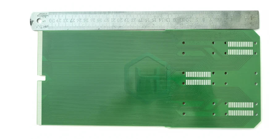
Ceramic PCB design requires careful consideration of thermal performance, mechanical stress, electrical requirements, and manufacturing limitations. A proper Design for Manufacturability (DFM) approach helps reduce production risks and improves long-term field reliability.
HILPCB works with customers during the design stage to optimize ceramic substrate selection, copper structures, interconnect layouts, and assembly requirements.
Key DFM Considerations
- Material Selection: Select Al₂O₃, AlN, or Si₃N₄ based on thermal conductivity, dielectric properties, mechanical strength, and cost requirements.
- Thermal Path Engineering: Optimize copper thickness, copper coverage, via structures, and substrate thickness to achieve efficient heat spreading.
- Line Width and Spacing: Match circuit geometry requirements with the resolution capability of the selected ceramic PCB process. DPC supports finer patterns, while DBC focuses on high-current structures.
- Via and Interconnect Design: Select appropriate filled vias, plated vias, or laser-drilled structures based on electrical current, thermal transfer, and mechanical requirements.
- Assembly Compatibility: Design solder pads and surface finishes to support reliable SMT assembly, wire bonding, and semiconductor attachment processes.
The HILPCB DFM review process evaluates electrical performance, mechanical stress, thermal behavior, and manufacturing feasibility before production begins. This approach helps ensure every project entering Ceramic PCB Fabrication achieves consistent quality and repeatable manufacturing results.
Partner with HILPCB Factory for One-Stop Ceramic and Electronic Manufacturing Solutions
HILPCB Factory provides ceramic PCB manufacturing together with complete PCB fabrication, assembly, and electronic manufacturing services. Our production capabilities support ceramic substrates, FR4 PCBs, Rogers high-frequency materials, metal-core PCBs, and flex-rigid PCB assemblies.
By combining fabrication, SMT assembly, through-hole assembly, and system integration services, HILPCB helps OEM customers reduce supply chain complexity and improve product consistency.
Our ceramic PCB solutions support applications including power modules, RF systems, LED electronics, automotive controllers, industrial equipment, and medical devices. From prototype development to volume manufacturing, we provide engineering support throughout the product lifecycle.
Why Engineers Choose HILPCB
- Comprehensive Manufacturing Capability: Ceramic PCB fabrication, PCB assembly, SMT, through-hole assembly, box build, and product integration services.
- Engineering Support: DFM and DFA assistance for high-power, high-frequency, and mixed-material electronic assemblies.
- Certified Quality Systems: Manufacturing processes aligned with ISO 9001, IATF 16949, and AS9100 requirements for automotive, aerospace, and medical applications.
- Global Production Support: Prototype development and scalable production with quality control and manufacturing traceability.
HILPCB Factory helps engineers develop reliable electronic products by combining ceramic PCB expertise with complete manufacturing capabilities.
Explore our ceramic substrate solutions on our Ceramic PCB Product Page or request a custom quote for your application.