
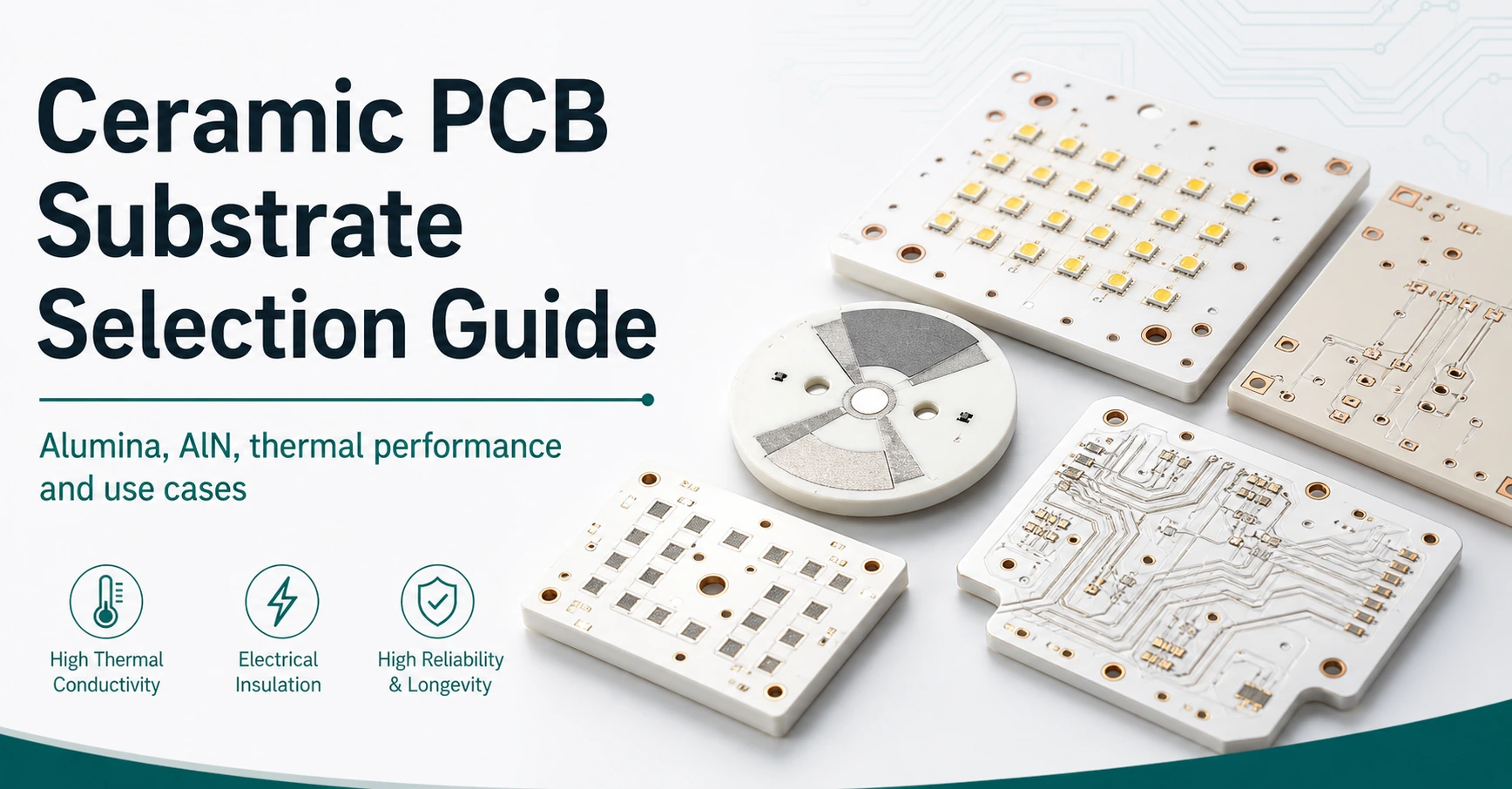
- Treat ceramic PCB substrate selection as a platform decision, not just a premium-material label to slap onto every hot board.
- Distinguish between material families (
alumina,AlN,Si3N4) and process lanes (DBC,DPC,AMB,LTCC,thin-film). They describe different levels of engineering decisions and should not be merged into one shorthand. - Default to Alumina (
Al2O3) as the practical first ceramic family when cost, electrical insulation, dimensional stability, and moderate thermal demand are balanced. - Escalate to Aluminum Nitride (
AlN) when higher thermal conductivity and closer CTE alignment to semiconductor devices justify the extra material cost and process control. - Keep
IMSand metal-core PCB routes in the comparison when the design simply needs a metal-base thermal platform rather than a true ceramic dielectric substrate.
A robust ceramic PCB selection review doesn't ask "Which ceramic sounds best?". It asks "What thermal, electrical, or mechanical constraint is forcing this board out of a conventional FR-4 or metal-core laminate route?" Once that constraint is defined, Alumina, AlN, DBC, and LTCC can be placed into their proper functional roles instead of being used as generic marketing buzzwords.
Search queries surrounding ceramic PCBs, alumina substrates, AlN, and DBC often treat all these terms as if they belong in the same bucket. They do not. Some queries are really asking about thermal management platforms for high-power LEDs. Others are about matching the CTE of bare bare dies in power semiconductor modules. Still others are asking about high-frequency RF performance or harsh environment reliability. This guide is only useful when it reduces this noise to a specific, board-level platform decision.
This decision isn't "what is the best ceramic PCB?" It's "which ceramic material and metallization process actually solves the heat flow, CTE, dielectric, or packaging problem for this specific assembly?"
This matters because ceramic PCB terminology drifts very easily. A weak draft lists every ceramic material and process as if any supplier can build any combination. A stronger draft narrows each acronym down until the reader can see its exact purpose. Alumina is useful when cost-accessible, moderately high thermal conductivity and electrical insulation are required. AlN is useful when the thermal flux is extreme and CTE matching to silicon is critical. DBC is a metallization choice for carrying heavy currents. LTCC is a co-fired process for complex RF or compact modules. None of these become more useful by being described as a universal thermal cure-all.
The safest way to organize this page is around the release responsibility. Before the board reaches the quote stage, the data package should already know:
- whether the design actually requires a ceramic dielectric, or if a metal-core PCB (MCPCB) would suffice
- whether Alumina is sufficient, or if the thermal/CTE demands strictly require AlN or Si3N4
- which metallization process (DBC, DPC, AMB, thick-film, thin-film) matches the copper thickness and fine-line geometry requirements
- what mechanical mounting and assembly constraints are placed on the brittle ceramic substrate
Once these answers are clear, the method choice becomes much sharper. Without them, the article turns into exactly what it should avoid: a broad glossary that names several materials but helps the reader decide nothing.
In This Guide
- What exactly is a ceramic PCB substrate?
- When should you choose a ceramic PCB instead of FR-4, IMS, or metal-core PCB?
- Alumina vs AlN vs Si3N4: Which ceramic substrate fits the board's thermal constraints?
- DBC, DPC, AMB, LTCC, thick-film, and thin-film: What process is really being selected?
- What design checks must be passed before releasing a ceramic PCB to manufacturing?
- What are the most common ceramic PCB failure modes and how can you prevent them?
- What drives the cost of a ceramic PCB and how can procurement balance the trade-offs?
- What should be included in an RFQ checklist for a ceramic PCB quote?
- FAQ
- Next steps
What exactly is a ceramic PCB substrate?
A ceramic PCB substrate is the insulating base of a circuit board when the base material is a ceramic rather than FR-4, polyimide, PTFE laminate, or an insulated metal substrate (IMS). In board-level reviews, the term usually points to alumina (Al2O3), aluminum nitride (AlN), silicon nitride (Si3N4), or a related ceramic platform with copper or other metallization added through a defined process.
That definition is intentionally narrow. It keeps ceramic PCB from becoming a loose marketing phrase. A ceramic board is not automatically an LTCC module, a thin-film circuit, a DBC power substrate, or a metal-core PCB. Those options may be related to the same design discussion, but they are not the same decision.
The first review question is therefore not “Which ceramic sounds best?” It is “What problem is forcing the board out of a conventional laminate route?” The answer usually sits in one of four areas: heat flow, coefficient of thermal expansion, dielectric/electrical behavior, or mechanical/package interaction. If none of those burdens is clear, the project may not yet need a ceramic PCB substrate.
The second review question is the level of naming. Ceramic substrate is a class term. Alumina and AlN are material-family terms. DBC, DPC, AMB, thick film, thin film, and LTCC are process or construction terms. IMS is a neighboring metal-base platform. Using the wrong level too early creates quotation errors, false expectations, and avoidable redesign.
| Term | What level it describes | Safe use in a release review | Common mistake |
|---|---|---|---|
| Ceramic substrate | Broad platform class | Use when the board is being reviewed as a ceramic-base platform | Treating it as if it already means alumina, AlN, DBC, or LTCC |
| Alumina / Al2O3 | Ceramic material family | Use when cost/performance balance and moderate-to-high thermal demand are under review | Calling every ceramic board an alumina PCB |
| AlN / aluminum nitride | Ceramic material family | Use when higher thermal conductivity and semiconductor package interaction justify review | Calling it universally “better” without cost, process, or reliability context |
| Si3N4 / silicon nitride | Ceramic material family | Use when fracture toughness and harsh power-module reliability are key considerations | Mentioning it as a standard option without supplier/process confirmation |
| DBC / DPC / AMB | Metallization or copper-ceramic process lane | Use only when the board construction actually needs that process | Listing all process names as if every supplier offers every route |
| LTCC | Co-fired ceramic process family | Use for multilayer co-fired ceramic structures and RF/package contexts | Using LTCC as a synonym for all ceramic PCBs |
| Thin-film ceramic | Fine-pattern ceramic metallization process family | Use for precision, RF, microwave, sensor, and package-style circuits where supported | Treating it as the same thing as generic AlN or alumina PCB |
| IMS / metal-core PCB | Metal-base thermal-management platform | Keep in scope when the board may need an insulated metal substrate rather than ceramic | Calling IMS a ceramic PCB because both are used for heat management |
The practical goal is to define the board platform before discussing fabrication. A phrase such as ceramic PCB fabrication is not quote-ready until the design team knows the ceramic family, process direction, copper requirement, surface finish, thickness target, tolerance burden, and inspection scope.
When should you choose a ceramic PCB instead of FR-4, IMS, or metal-core PCB?
Choose a ceramic PCB substrate when the board-level burden is tied to ceramic-specific behavior: high thermal conductivity through an electrically insulating base, stable performance at elevated temperature, low moisture absorption, high dielectric strength, or closer thermal-expansion compatibility with a device package. Do not choose ceramic only because the product is high power or premium. High-power boards can also belong on heavy copper, metal-core, IMS, high thermal PCB, or hybrid stackup routes.
A good selection review starts by keeping alternatives alive long enough to reject them for a specific reason. If the design can meet the thermal and electrical target with FR-4, high-Tg FR-4, heavy copper, thermal vias, or a localized heat spreader, ceramic may add cost and mechanical risk without enough benefit. If the dominant need is a metal base that spreads heat laterally under insulated copper circuitry, a Metal Core PCB or broader IMS review may be more accurate than a ceramic route. If the dominant issue is insertion loss, dielectric constant, or RF layout rather than heat flow through a ceramic base, a High Frequency PCB review may be the better starting point.
Ceramic becomes more defensible when the design needs both electrical insulation and a direct heat path through the substrate. LED modules, power semiconductor substrates, RF power modules, laser drivers, UV equipment, high-voltage power conversion, sensors, and compact automotive or industrial electronics are typical review contexts. The final decision still depends on layout geometry, copper thickness, assembly method, mechanical mounting, and thermal cycling risk.
Decision Matrix: When to Escalate to Ceramic Substrates
| Board burden | Route that should stay in scope | When ceramic becomes more defensible | When ceramic may be premature |
|---|---|---|---|
| General heat reduction | Heavy copper, thermal vias, high thermal PCB, IMS | Heat must move through an electrically insulating substrate with lower thermal resistance | Thermal target can be met through copper area, heatsink design, or standard laminate changes |
| Power module / die attach style assembly | DBC, AMB, DPC ceramic, power substrate | Copper-to-ceramic structure is central to current carrying and thermal path | The board is only a standard SMT PCB with a few hot components |
| Cost-sensitive LED or industrial board | Alumina PCB, IMS, metal-core PCB | Electrical insulation and ceramic stability matter, but AlN cost is not justified | Metal-core provides the needed thermal path with lower complexity |
| High heat flux near semiconductor package | AlN ceramic substrate, AMB/DBC where applicable | Higher thermal conductivity and CTE direction are central to the package interface | Heat source can be moved, derated, or handled by package/heatsink changes |
| RF or microwave precision | High-frequency laminate, thin-film ceramic, LTCC | Ceramic process supports the required geometry, loss behavior, and package style | The design is a conventional RF PCB where Rogers/PTFE-type laminate is sufficient |
| Harsh thermal cycling | Ceramic family and process with reliability data; sometimes Si3N4 route | Substrate fracture toughness and copper-ceramic fatigue must be engineered | Ceramic is selected without thermal-cycle, mounting, or depanelization control |
A ceramic PCB selection review should end with a sentence that a fabricator can act on. “Use ceramic” is not enough. “Evaluate an alumina DBC substrate with defined copper thickness for this power module geometry” is much stronger. “Evaluate AlN ceramic because the package heat flux and CTE target cannot be met by alumina or IMS” is stronger still.
Alumina vs AlN vs Si3N4: Which ceramic substrate fits the board's thermal constraints?
Alumina and AlN are the two ceramic families most teams compare first. Silicon nitride appears in high-reliability power-module conversations, but it should be handled as a supplier- and process-specific option rather than a default replacement for alumina or AlN.
Alumina (Al2O3) is usually the practical ceramic baseline. It is widely used, electrically insulating, mechanically strong, and more cost-accessible than AlN in many board programs. Published supplier data often places alumina substrate thermal conductivity around the low-to-mid 20 W/m·K range for common electronics grades, but the actual value depends on purity, formulation, thickness, surface finish, and the supplier’s data sheet. That is already far above FR-4, but it is not in the same thermal class as AlN.
Aluminum Nitride (AlN) is the higher-thermal ceramic direction. Supplier examples commonly list AlN substrate thermal conductivity around 170 W/m·K for certain electronics substrate grades. AlN can also offer a CTE direction closer to silicon than alumina in many package-level comparisons. Those strengths are why AlN belongs in high heat-flux, power semiconductor, laser, RF power, and compact thermal-path reviews. The trade-off is cost, availability, process sensitivity, and the need to verify metallization, copper adhesion, and reliability for the exact construction.
Silicon Nitride (Si3N4) is often discussed when the review is less about maximum thermal conductivity alone and more about mechanical robustness and thermal cycling reliability in demanding power modules. It can be a strong direction for certain traction inverter, EV power, or high-reliability module applications, but it should not be inserted casually into a standard ceramic PCB quote without confirming supplier capability and process route.
| Ceramic family | Typical review reason | Directional property notes | Good-fit examples | Procurement caution |
|---|---|---|---|---|
| Alumina / Al2O3 | Balanced ceramic route for cost, insulation, stability, and moderate thermal demand | Common published electronics substrate examples are around 20–30 W/m·K; lists ~24 W/m·K, 500 MPa flexural strength | LED substrates, industrial power boards, sensors, hybrid circuits, cost-sensitive ceramic boards | Confirm purity, thickness, copper process, tolerances, and whether DBC/DPC/thick-film is intended |
| Aluminum nitride / AlN | Higher thermal conductivity and package-interaction direction | Supplier examples commonly list around 170 W/m·K for AlN substrate products; lists 450 MPa bending strength | Power modules, RF power, laser drivers, compact high-heat devices, semiconductor-adjacent assemblies | Higher cost and process sensitivity; confirm metallization, solderability, copper adhesion, and reliability data |
| Silicon nitride / Si3N4 | Thermal cycling and mechanical toughness direction for demanding power modules | Published power-substrate data sheets often position Si3N4 for robustness and reliability rather than only maximum thermal conductivity | EV power modules, traction inverters, harsh thermal-cycle substrates | Not always a standard ceramic PCB option; confirm availability, process route, and design rules early |
This table is not a universal ranking. It is a release-review filter. The right substrate is the one whose material behavior solves the board’s dominant constraint with a process route the supplier can actually build and test.
For many projects, the first clean decision is not alumina versus AlN. It is ceramic versus non-ceramic. Once ceramic is justified, the second decision is alumina versus AlN versus another ceramic family. Only after that should the discussion move into DBC, DPC, AMB, LTCC, thick film, or thin film.
DBC, DPC, AMB, LTCC, thick-film, and thin-film: What process is really being selected?
Ceramic PCB fabrication is not one process. It is a family of possible substrate and metallization routes. A quote request that says only “ceramic PCB” forces the supplier to guess whether the design needs thick copper for current, fine traces for RF, multilayer co-fired ceramic, direct plated copper, or a simple ceramic substrate with metallization.
DBC, DPC, and AMB are often seen in ceramic power-substrate discussions. LTCC and HTCC belong to co-fired ceramic structures. Thick-film and thin-film ceramic describe different metallization and patterning approaches. These terms are useful only when they are tied to the board’s real construction need.
Decision Matrix: Ceramic Metallization Processes
| Process / route | What it usually means in selection language | Where it often fits | What to confirm before quote |
|---|---|---|---|
| DBC / Direct Bonded Copper | Copper bonded directly to ceramic, often used for power substrates and thicker copper needs | Power modules, IGBT/MOSFET substrates, high-current thermal paths | Ceramic type, copper thickness, isolation voltage, outline method, solder mask/finish, thermal cycling requirement |
| DPC / Direct Plated Copper | Metallization and plated copper route that can support finer patterns than many thick-copper routes | LEDs, sensors, RF/power hybrid circuits, fine-feature ceramic boards | Minimum trace/space, copper thickness, via method, adhesion test, plating reliability |
| AMB / Active Metal Brazing | Ceramic-to-copper joining route used in demanding power substrates, often discussed with AlN or Si3N4 | High-reliability power modules and harsh thermal cycling contexts | Ceramic family, copper thickness, braze system, thermal cycling data, peel strength acceptance |
| Thick-film ceramic | Screen-printed conductive/resistive pastes fired on ceramic | Hybrid circuits, power resistors, sensors, rugged electronics | Paste system, fired thickness, line width, resistance tolerance, trimming needs |
| Thin-film ceramic | Vacuum-deposited or precision metallized thin films on ceramic | RF/microwave, sensors, packages, fine-line precision circuits | Metallization stack, line/space, adhesion, surface roughness, controlled impedance expectations |
| LTCC | Low Temperature Co-Fired Ceramic multilayer process | RF modules, packages, compact multilayer passive/interconnect structures | Layer count, via fill, conductor metal, shrinkage tolerance, co-fired material system |
A practical review should avoid process stacking. A sentence such as “We can make ceramic PCBs with DBC, DPC, AMB, LTCC, thick film, and thin film” looks comprehensive, but it is not helpful unless the board has a reason to choose one path. Better release language says: “This design is being quoted as alumina DPC because fine traces and moderate copper thickness matter more than high-current DBC copper.” Or: “This module should stay in AlN DBC/AMB review because heat flux and solder-layer fatigue dominate the risk.”
The process choice also affects what design data the supplier needs. DBC and AMB discussions require more attention to copper thickness, ceramic thickness, thermal cycling, partial discharge or high-voltage behavior where applicable, and mechanical stress. DPC and thin-film discussions require more attention to fine features, metallization stack, plating adhesion, surface roughness, and RF or sensor tolerances. LTCC discussions require early layer planning because shrinkage and co-firing constraints are not the same as ordinary multilayer PCB lamination.
What design checks must be passed before releasing a ceramic PCB to manufacturing?
Ceramic boards fail differently from FR-4 boards. They do not have the same flex margin, and they make mechanical decisions visible. A release review should therefore include mechanical, thermal, electrical, and manufacturing checks before the quote package is frozen.
The mechanical review is the part most teams underestimate. Ceramic substrates can crack from panel handling, aggressive depanelization, clamp pressure, screw torque, uneven heatsink contact, or board flex during assembly. A design that would survive as FR-4 may be unsafe as ceramic if mounting holes, edge clearances, panel tabs, or fixture loads are copied without review.
The thermal review must identify the real heat path. Ceramic helps when heat moves through the substrate into a baseplate, heatsink, or package interface. If the thermal model assumes heat magically disappears after entering the ceramic, the design is not ready. The stack should define heat source location, copper thickness, ceramic thickness, interface material, baseplate, airflow or liquid cooling condition, and allowable component temperature.
The electrical review should separate insulation from signal behavior. Alumina and AlN can provide strong electrical insulation, but the board still needs spacing, creepage/clearance, via strategy, copper edge control, solder mask decisions, and finish selection. RF or microwave designs need dielectric, roughness, and patterning review rather than a generic ceramic claim.
| Review gate | What to check | Practical release question |
|---|---|---|
| Platform justification | Why ceramic is needed instead of FR-4, IMS, metal-core, or high thermal PCB | What failure or margin problem does ceramic solve? |
| Ceramic family | Alumina, AlN, Si3N4, or another ceramic family | Is this a cost/performance choice, a high-thermal choice, or a mechanical-reliability choice? |
| Metallization process | DBC, DPC, AMB, thick film, thin film, LTCC, or supplier-defined route | Does the process match copper thickness, feature size, and thermal cycling needs? |
| Outline and depanelization | Routing, laser cutting, scoring restrictions, edge quality | Can the outline be made without hidden cracks or stress concentration? |
| Mounting and assembly | Screw torque, clamp pressure, heatsink flatness, fixture loading | Where can ceramic flex or point load occur during assembly? |
| Inspection and test | AOI, electrical test, adhesion, microsection, thermal cycling, X-ray where relevant | Which risks must be verified before production release? |
A ceramic release package should include explicit “do not assume FR-4 handling” notes when assembly partners are not familiar with ceramic. This is especially important for depanelization, screw torque, heatsink attachment, and rework. Localized bending during manual handling can be enough to create latent defects that appear only after thermal cycling.
What are the most common ceramic PCB failure modes and how can you prevent them?
A stronger ceramic PCB article should not only describe material benefits. It should also say where ceramic boards most often get into trouble. The risks below are not exotic; they are the everyday problems that appear when substrate, copper, process, and assembly decisions are not reviewed together.
| Failure mode | Likely cause | Early warning sign | Prevention / review action |
|---|---|---|---|
| Ceramic cracking or edge chipping | Aggressive depanelization, sharp internal corners, poor handling, point loading | Chips at outline, inconsistent edge quality, cracks after assembly | Use low-stress routing/laser where appropriate, add radii, review panel tabs, define handling and inspection notes |
| Copper-to-ceramic delamination | Wrong process for copper thickness, poor adhesion control, thermal cycling stress | Peeling, blistering, high resistance, local overheating | Specify process route, copper thickness, adhesion/peel test requirement, and thermal-cycle validation where needed |
| Solder joint fatigue | CTE mismatch, stiff assembly, high temperature swing | Cracked solder near high-power packages or connectors | Review package CTE, solder alloy, pad design, heatsink flatness, and thermal cycling profile |
| Hot spot remains after ceramic upgrade | Heat source not coupled to thermal path, insufficient copper spreading, poor TIM/baseplate design | Component temperature does not improve as expected | Model full thermal path: die/package, copper, ceramic, interface, baseplate, heatsink, airflow |
| High-voltage insulation weakness | Inadequate spacing, contamination, edge metallization, poor creepage/clearance planning | Leakage, partial discharge risk, field failure under humidity or voltage stress | Define voltage, creepage/clearance, cleanliness, conformal coating/potting, and test condition |
| Warpage or assembly flatness issue | Copper imbalance, large copper islands, uneven thermal mass, fixture stress | Poor solder paste contact, uneven bondline, assembly yield loss | Balance copper where possible, review panel support, define flatness requirement and assembly fixture plan |
The most important habit is to define the failure mode the ceramic substrate is supposed to prevent. If the board is being changed to ceramic to reduce temperature, measure temperature. If the purpose is power cycling reliability, define cycling conditions. If the purpose is RF precision, define the transmission-line and test expectations. Without a measurable objective, ceramic selection becomes a material substitution rather than an engineering decision.
What drives the cost of a ceramic PCB and how can procurement balance the trade-offs?
Ceramic PCB cost is driven by more than material name. Alumina is usually less costly than AlN for comparable board complexity, but the final quote can change quickly when copper thickness, ceramic thickness, process route, tolerance, surface finish, test burden, outline complexity, and panel utilization change.
The biggest quote drivers are usually these: ceramic family, metallization process, copper thickness, ceramic thickness, minimum line/space, via requirements, outline method, yield-sensitive tolerances, thermal cycling or high-voltage testing, and documentation requirements. For small prototypes, tooling, setup, and supplier engineering time can dominate. For production, yield, panel utilization, process stability, and inspection coverage become more important.
The lowest total cost is rarely the lowest material price. A cheaper substrate that fails thermal cycling, cracks at assembly, or requires a late process change is not cheaper at program level. A good procurement decision weighs first-article risk, supplier process fit, and quote clarity alongside unit price.
What should be included in an RFQ checklist for a ceramic PCB quote?
A ceramic PCB quote is much more accurate when the request separates fixed requirements from open trade-offs. If the supplier has to infer the ceramic family, copper thickness, process route, and test scope, the quote will either be padded with assumptions or priced too narrowly to be safe.
Use the checklist below when sending data to HILPCB or comparing ceramic PCB suppliers.
General Design & Stackup
- Design files: Gerber/ODB++/IPC-2581, drill files, netlist, fabrication drawing, assembly drawing if applicable. Include revision number and units.
- Stackup intent: Ceramic family (Alumina, AlN, etc.), ceramic thickness target, copper thickness, number of copper layers. Mark unknown items as “open for supplier recommendation”.
- Process direction: DBC, DPC, AMB, LTCC, thick-film, thin-film, or “supplier to recommend”.
Mechanical & Thermal
- Thermal data: Heat source location, power dissipation, max component temperature, heatsink/baseplate interface, ambient condition. A simple thermal sketch is incredibly useful.
- Mechanical data: Board outline, mounting holes, torque limits, fixture constraints, flatness, edge quality, keepouts. Ceramic cracking risk often starts here.
Assembly & Validation
- Electrical requirements: Operating voltage, isolation voltage, creepage/clearance, impedance targets, RF frequency if relevant.
- Assembly data: SMT/BGA/wire bonding, solder alloy, reflow profile constraints, underfill/potting, heatsink attachment. State whether the board will be assembled by HILPCB or another partner.
- Surface finish: ENIG, immersion silver, OSP, wire-bondable finish, solderable metallization, or supplier recommendation.
- Reliability / test: Electrical test, AOI, X-ray, microsection, peel/adhesion, thermal cycling, high-voltage test, cleanliness. Define acceptance criteria when possible.
A strong RFQ does not need every answer on day one. It needs to show which decisions are fixed, which decisions are open, and which risks must be resolved before release. That lets the supplier respond with a manufacturable stackup instead of a generic ceramic PCB price.
FAQ
Is a ceramic PCB the same thing as an alumina PCB?
No. Ceramic PCB is the broader platform term. Alumina PCB is one ceramic PCB family based on aluminum oxide (Al2O3). A ceramic PCB could also involve AlN, Si3N4, LTCC, thin-film ceramic, or another ceramic route depending on the construction.
Is AlN always a better substrate choice than alumina?
No. AlN is usually the higher-thermal direction, but it is not automatically the better business or engineering choice. Alumina can be the better fit when thermal density is moderate, cost matters, and the design does not need the higher thermal conductivity or package CTE direction of AlN.
What is the biggest mistake made during ceramic PCB selection?
The biggest mistake is mixing class, material, and process language. A design that says only “ceramic PCB” has not specified whether it needs alumina, AlN, DBC, DPC, AMB, LTCC, thin film, thick film, or another route.
Is LTCC considered a type of ceramic PCB?
LTCC is a low-temperature co-fired ceramic process family. It is related to ceramic circuit technology, but it should not be used as a blanket synonym for ceramic PCB, alumina PCB, AlN substrate, or DBC substrate.
When should IMS or metal-core PCBs stay in the comparison against ceramic?
IMS or metal-core PCB should stay in the comparison when the board mainly needs a metal-base thermal platform with an insulated dielectric layer. Ceramic should be selected only when the board needs ceramic-specific insulation, thermal, CTE, or package behavior.
What information does a PCB manufacturer need for an accurate ceramic PCB quote?
A supplier needs Gerber or ODB++ data, stackup intent, ceramic family, copper thickness, process direction, surface finish, voltage and thermal requirements, mechanical mounting constraints, assembly method, test requirements, quantity, and lead-time target.
Can switching to a ceramic PCB prevent all thermal failures?
No. Ceramic can reduce part of the thermal resistance when used correctly, but the full heat path still includes the package, copper, ceramic thickness, interface material, baseplate, heatsink, airflow, and assembly quality.
Should Beryllium Oxide (BeO) be used for new ceramic PCB designs?
BeO should not be treated as a default new-design option. It may appear in legacy or specialized high-thermal applications, but safety, handling, and compliance controls must be explicitly reviewed before it enters a design or quotation.
Next steps
If your current board is being pushed toward ceramic because of heat, voltage, package CTE, or reliability risk, do not start with a generic material request. Start with a review package that explains what the ceramic substrate must solve and which trade-offs are still open.
Send the Gerber package, stackup intent, copper requirement, thermal load, mechanical outline, assembly method, and test expectations to [email protected], or upload the project through the Quote page. For an early-stage project, ask for a substrate/process recommendation. For a release-stage project, ask for a manufacturability review that confirms ceramic family, process route, inspection scope, and quote assumptions before the design is frozen.
Which reference standards apply to ceramic PCB manufacturing?
Ceramic PCB selection can support product safety, reliability, and compliance, but it does not by itself certify the final product. Final electrical safety, EMC, thermal safety, automotive, medical, aerospace, and environmental compliance must be verified at the product or system level by the customer and the appropriate test laboratory.
Common reference standards and specifications used during PCB/PCBA review may include:
- IPC-A-600 — IPC
- IPC-6012 — IPC
- IPC-A-610 — IPC
- IPC-TM-650 — IPC
- UL 796 — UL Solutions
- UL 94 — UL Solutions
- ISO 9001:2015 — ISO
- ISO 13485:2016 — ISO
- IATF 16949 — IATF
- RoHS — European Union
- REACH — European Union
Use these as review references. The applicable standard depends on the product, market, voltage, environment, customer specification, and supplier certification scope.