
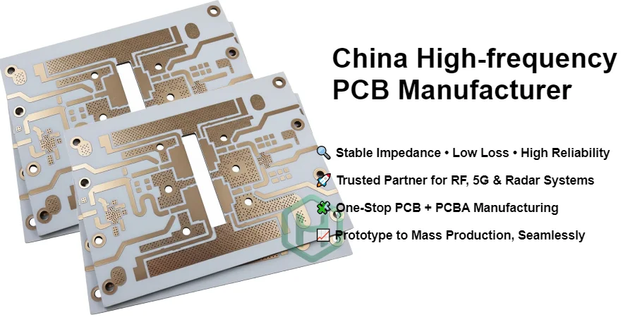
In RF, microwave and high-speed digital systems, the PCB is an active RF component, not just a mechanical carrier. Once frequency, edge rate and dynamic range go beyond what standard FR-4 can support comfortably, you must start thinking in terms of low-loss PCB boards, impedance-matching PCBs, and controlled high-frequency multilayer PCB production instead of “just another four-layer board”.
This article looks at high-frequency boards from the perspective of a China high-frequency PCB manufacturer and microwave PCB supplier: what really defines performance, which technical requirements and quality standards matter, what typical common issues look like, and how all of this ties into long-term high-frequency PCB competitiveness.
1. Performance core: low-loss behaviour and impedance-matching PCBs
For high-frequency and microwave designs, two characteristics dominate PCB behaviour:
- Low-loss signal transmission
- Controlled impedance and matching
1.1 Low-loss PCB boards
A genuine low-loss PCB board is the result of several coordinated decisions, not just a laminate choice:
- Dielectric system: stable Dk and low Df over the operating band, with known variation versus frequency and temperature.
- Copper and plating: appropriate copper roughness and plating thickness so conductor loss does not dominate the budget at high frequency.
- Geometry and finish: line width, spacing and surface finish (ENIG, immersion silver, OSP, etc.) selected with insertion loss and skin-effect in mind.
A professional high-speed PCB manufacturer will treat loss targets as hard constraints and recommend material stacks and geometries that realistically meet them, instead of simply quoting “FR-4 vs RF material”.
1.2 Impedance-matching on the PCB
A true impedance-matching PCB is more than “50 Ω traces everywhere”:
- Stackup-driven impedance: trace widths are calculated from the actual stackup (dielectric thickness, Dk, copper thickness), not generic tables.
- Launch and transition control: vias, pads and connector launches are designed as part of the impedance path, not as afterthoughts.
- Tolerance windows: manufacturing tolerances for geometry and thickness are tied directly to the allowed impedance window.
From the manufacturer’s side, these are formal high-frequency PCB technical requirements, used to set up imaging, etching and lamination processes, not just optional “design notes”.
2. High-frequency multilayer PCB production and mixed material stacks
Most real-world high-frequency boards are multilayer and use more than one material family. Robust high-frequency multilayer PCB production is about making that complexity repeatable.
2.1 Stackup as a system, not as a drawing
A capable China high-frequency PCB manufacturer will:
- Place RF and microwave layers on low-loss laminates for critical transmission lines and sensitive analog sections.
- Reserve other layers (logic, low-speed I/O, power) for FR-4 or high-Tg FR-4, reducing cost without polluting the RF environment.
- Design via structures, back-drilling, and controlled depth features as part of the stack, not as isolated operations.
The stackup is treated as part of the circuit and as part of the process window at the same time. If it cannot be built reliably, it will not deliver reliable RF performance.
2.2 Hybrid and mixed-material architectures
In many designs, RF sections share a board or a board-set with high-speed digital interfaces and power conversion. That means mixed-material stacks and board-sets are common:
- RF laminates + FR-4 in one stackup
- Separate RF modules and digital carrier boards connected via high-speed links
- Combinations of microwave, high-speed and power boards in a single system
A competent microwave PCB supplier has to manage:
- CTE differences and lamination parameters between materials
- Long-term via reliability through mixed dielectrics
- Consistency of thickness, Dk and loss from lot to lot
Without this, the same Gerbers can yield different electrical behaviour in different production runs.
3. High-frequency board quality standards and formal technical requirements
To make performance stable rather than accidental, you need explicit high-frequency board quality standards that are linked to production data.
3.1 Defining measurable standards
Typical items in a technical and quality specification include:
- Impedance windows for each line class (e.g. 50 Ω microstrip ±10%, 100 Ω differential ±8%).
- Loss limits (e.g. maximum insertion loss per inch at a given frequency).
- Dimensional tolerances on line width, spacing, dielectric thickness and via registration.
- Surface requirements for flatness, coplanarity and plating in RF connector areas.
These form the backbone of a serious high-frequency PCB technical requirements document. The more explicitly they’re defined, the easier it is for the factory to control and for you to audit.
3.2 Process and quality integration
Inside a mature China high-frequency PCB manufacturing enterprise, these requirements are integrated into:
- Process capability studies on critical dimensions.
- Controlled imaging and etching recipes for RF layers.
- Documented lamination and drilling parameters specific to RF material stacks.
- Tailored electrical test strategies (including impedance coupons or RF patterns where needed).
This is where quality standards move from PowerPoint slides into the actual production floor.

4. High-frequency PCB common issues and the role of factory engineers
Even with good stackups and standards, there are recurring high-frequency PCB common issues that show up in the field when design and manufacturing are not properly aligned.
4.1 Typical failure or deviation patterns
Some of the most frequent issues:
- Impedance drift from batch to batch due to uncontrolled line width or dielectric thickness.
- Higher than expected loss, often related to rough copper use on critical layers, neck-downs at via transitions or over-etched fine lines.
- Via reliability problems in thick or hybrid stacks, especially after repeated thermal cycling or aggressive assembly profiles.
- Launch and connector anomalies, where connectors, shields or mechanical fixtures detune the local RF environment.
These problems are predictable when you’ve seen enough designs; they are also avoidable when a manufacturer’s engineering team is involved early.
4.2 High-frequency PCB engineers and consulting as part of the service
A serious manufacturer will have internal high-frequency PCB engineers who support customer projects as part of high-frequency PCB consulting, for example by:
- Comparing materials and stackups for specific bands, loss targets and environment classes.
- Translating S-parameter and timing requirements into geometry, tolerance and test constraints.
- Reviewing launch structures, via strategies and routing topologies with both performance and yield in mind.
- Identifying risky assumptions in the layout before they become expensive iterations on the bench.
When you choose a microwave PCB supplier or high-speed PCB manufacturer, access to this kind of engineering support is often more important than the nominal feature size on a capability table.
5. Quotation, lifecycle economics and high-frequency PCB competitiveness
A meaningful high-frequency PCB quotation is not just a number – it is a reflection of how the supplier understands your requirements and risk profile. Long-term high-frequency PCB competitiveness is about lifecycle economics, not just the cheapest first prototype.
5.1 What should go into a quotation request
To get a realistic quote and useful feedback, your RF or high-speed team should share:
- Target frequency bands and main application (radio, radar, test & measurement, backhaul, etc.).
- Preliminary stackup concept and material preferences (or constraints).
- Impedance classes and key loss budgets.
- Expected production pattern: one-off build, recurring small batches, or path to higher volume.
- Whether you need bare boards only or boards plus assembly and test.
This allows the manufacturer to size the process correctly and to propose options, not just a single price.
5.2 Competitiveness beyond unit cost
Real high-frequency PCB competitiveness includes:
- Technical robustness: the board behaves as simulated and stays inside defined windows over time.
- Process stability: the same design moves smoothly from prototype to recurring small batches and, if needed, larger runs without re-qualification.
- Engineering responsiveness: issues and questions are answered by experienced high-frequency PCB engineers, not only by sales.
- Total cost of ownership: fewer re-spins, less field failure risk, faster bring-up and shorter debug cycles.
In other words, a strong high-frequency PCB manufacturer is one that helps you hit your RF, schedule and cost targets over the entire life of the product—not only on the first order.
When you evaluate a microwave PCB supplier or high-speed PCB manufacturer, look beyond basic capability lists. Ask how they define and control low-loss behaviour, impedance, multilayer stackups, quality standards and common issue patterns. A China high-frequency PCB manufacturer that can clearly articulate these aspects—and back them up with engineering support and transparent quotations—is far more likely to be the kind of long-term partner your RF and high-speed products actually need.