
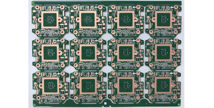
A consumer electronics PCB is a circuit board optimized for compact packaging, fast interfaces, wireless connectivity, controlled power use, manufacturability, and cost at the product's expected volume. The right construction depends on the enclosure, component packages, interfaces, thermal path, reliability target, and test strategy—not on the product category alone.
Key Takeaways
- Use HDI only where package escape, board area, or layer-transition density requires microvias.
- Choose rigid, flex, or rigid-flex construction from mechanical movement and assembly needs, not from a preference for thinner hardware.
- Define controlled-impedance, antenna, power, and thermal requirements before the stack-up is released.
- Design inspection and functional test access before dense placement removes it.
- Quote the board with the enclosure, cable, battery, display, antenna, and operating profile that affect final performance.
Which PCB Construction Fits the Product?
Consumer products compete for board area while combining processors, memory, radios, sensors, displays, batteries, and connectors. The smallest manufacturable solution is usually better than the most complex available solution. Home multimedia hardware follows the same logic: a DVD player PCB combines video decoding, audio output, and disc control on a cost-driven board.
| Product or constraint | Likely construction | Main decision drivers |
|---|---|---|
| Earbuds, audio modules, simple controls | 2–6 layer rigid PCB | Low noise, compact outline, cost, battery and connector layout |
| Smart-home hub or camera | 4–8 layer mixed-signal PCB | Ethernet or wireless RF, image or audio data, power and EMC |
| Smartphone, tablet, compact computer | Multilayer HDI PCB | Fine-pitch BGA escape, microvias, via-in-pad, high-speed interfaces |
| Smartwatch or body-worn device | Flex or rigid-flex | Curved packaging, low mass, sensor placement, controlled bend zones |
| Game console or graphics hardware | Multilayer rigid PCB | High-current PDN, memory interfaces, cooling and connector bandwidth |
| Camera, drone, or AR hardware | HDI or rigid-flex | Low mass, vibration, sensors, RF/GNSS, image-processing bandwidth |
Do not select layer count from a generic table. Start with package fan-out, reference-plane continuity, power distribution, isolation, shielding, routing density, board thickness, and assembly access. A HDI PCB can reduce area, but sequential lamination, filled microvias, and tighter registration add cost and reliability constraints. A rigid-flex PCB can remove connectors, but its bend zones, coverlay, stiffeners, and assembly carriers must be released as part of the design.
What Design Decisions Matter Most?
High-speed links need a stack-up with known dielectric properties, continuous reference planes, controlled impedance, and transitions that preserve return current. State interface-specific targets and tolerances on the drawing; "high speed" is not a fabrication requirement.
Power and thermal design are equally important. Define peak and average current by operating mode, battery and charging faults, allowable rail ripple, copper temperature rise, component limits, enclosure temperature, airflow, and contact to spreaders or chassis. High-Tg material can improve thermal robustness, but Tg is not thermal conductivity and does not replace a complete heat path.
Wireless performance belongs to the final product. Keep antenna zones clear, control RF feed impedance, provide a tunable matching network, and verify the radio with the production enclosure, display, battery, cables, and user-proximity condition. A bare-board RF check cannot predict every installed detuning effect.
For flex products, classify each region as static, service-flex, or dynamic. Keep vias, component pads, stiffener edges, and abrupt trace-width changes out of repeated bend zones. Validate the released material stack and bend profile rather than relying on one universal bend-radius rule.
How Should Materials and Finishes Be Selected?
Standard FR-4 is suitable for many consumer products. Higher-Tg or lower-loss material is justified when the assembly profile, operating temperature, interface loss budget, thickness control, or reliability model requires it. Use the laminate supplier's current data and the fabricator's pressed-thickness model for impedance work.
Surface finish follows component pitch, solderability, shelf life, wire bonding if applicable, contact function, and cost. ENIG is flat and common for fine-pitch assembly; OSP can be economical for suitable lead-free processes; immersion silver or ENEPIG may fit specific RF, contact, or bonding requirements. State thickness and acceptance requirements when they matter.
How Should Assembly and Test Be Planned?
Fine-pitch QFNs, BGAs, 0201-class passives, shields, cameras, connectors, and flex tails create interacting stencil, placement, reflow, warpage, cleaning, and inspection risks. The assembly plan should define paste inspection, AOI, X-ray coverage, rework limits, moisture handling, programming, functional test, and serialization by package and risk.
| Failure mode | Common cause | Prevention or evidence |
|---|---|---|
| BGA opens or head-in-pillow | Package or board warpage, weak paste transfer, poor profile | Package review, stencil and profile validation, X-ray plus functional evidence |
| QFN thermal-pad voiding | Paste-window and gas-release behavior | Package-specific stencil study, profile control, agreed X-ray method and limits |
| Intermittent flex connection | Stress at bend, stiffener, pad, or connector transition | Bend-zone review, strain relief, representative flex and assembly testing |
| Radio range loss | Antenna detuning, poor keepout, enclosure or cable coupling | Installed-state tuning and conducted/radiated verification |
| Reset, noise, or display artifacts | PDN impedance, return-path discontinuity, EMI coupling | Load-state measurement, layout review, pre-compliance and functional tests |
| Early field failure | Uncontrolled substitution or weak change control | Approved alternates, revision traceability, first-article and requalification rules |
What Drives Cost?
The main recurring drivers are board area and panel utilization, layer count, sequential-lamination cycles, microvia type, filled via-in-pad, line and registration limits, material, surface finish, controlled impedance, flex construction, component mix, inspection, and test time. Non-recurring cost includes fixtures, programs, carriers, stencils, SI or RF work, and qualification builds.
Spend where the risk model needs evidence. Extra layers may be cheaper than an unnecessarily aggressive microvia stack; a functional fixture may cost more up front but prevent repeated manual diagnosis during ramp.
Consumer Electronics PCB RFQ Checklist
- Schematics, fabrication and assembly data, BOM with approved alternates, stack-up, impedance table, mechanical files, and revision history
- Package data, minimum features, via structure, board thickness, finish, controlled-depth drilling, flex zones, stiffeners, and panel constraints
- Interface speeds, antenna and matching requirements, power tree, battery and charging states, current loads, thermal limits, and enclosure conditions
- Solder alloy, cleanliness, coating or shielding, moisture handling, cosmetic criteria, rework limits, and first-article requirements
- SPI, AOI, X-ray, electrical test, programming, calibration, functional-test limits, fixtures, sample plans, and retained records
- Prototype and production quantities, forecast, serialization, packaging, change notification, and requalification triggers
Reference Standards and Responsibility Scope
- IPC-2221 — IPC
- IPC-2222 — IPC
- IPC-2223 — IPC
- IPC-2226 — IPC
- IPC-6012 — IPC
- IPC-6013 — IPC
- IPC-A-610 — IPC
- IPC J-STD-001 — IPC
Confirm the current revision, product class, regional requirements, and customer-specific precedence. HILPCB can fabricate and assemble the released board and provide contracted inspection and test evidence. The product owner retains responsibility for enclosure mechanics, battery safety, radio and EMC approval, software and cybersecurity, user-contact materials, system reliability, and final market compliance unless explicitly assigned.
Why Build With HILPCB?
HILPCB can review consumer-electronics projects across stack-up, DFM, fabrication, sourcing, SMT and THT assembly, inspection, programming, and functional-test planning. The useful comparison between suppliers is the written process and evidence offered for your exact construction—not a generic promise of advanced equipment or high yield.
Frequently Asked Questions
Does every compact consumer product need HDI?
No. HDI is justified when fine-pitch package escape, routing density, board area, or interconnect length cannot be met economically with through vias. A conventional multilayer board is simpler when it satisfies the design.
When should a product use rigid-flex instead of connectors?
Use rigid-flex when packaging, mass, repeated assembly, signal continuity, or reliability supports the added fabrication complexity. Compare it with separate rigid boards and qualified connectors at the complete product level.
Is ENIG always the best surface finish?
No. ENIG is flat and widely used for fine-pitch assembly, but OSP, immersion silver, ENEPIG, or other finishes may better fit cost, RF, bonding, shelf-life, or contact requirements.
Which inspections are needed for dense consumer PCBAs?
Choose inspection by defect visibility and risk. SPI controls paste, AOI sees accessible joints and placement, and X-ray adds evidence for hidden joints. Electrical and functional tests are still required for faults images cannot prove.
What information most improves quote accuracy?
The released stack-up, package and via details, enclosure constraints, approved BOM, interface and impedance requirements, test limits, production volume, and change-control expectations remove the most quotation assumptions.
Release the Evidence With the Design
A consumer electronics PCB succeeds when density, signal integrity, power, RF, mechanics, assembly, and test are resolved as one product. Send HILPCB the released board package plus the installed operating and acceptance conditions so the quotation reflects the hardware you intend to ship.