
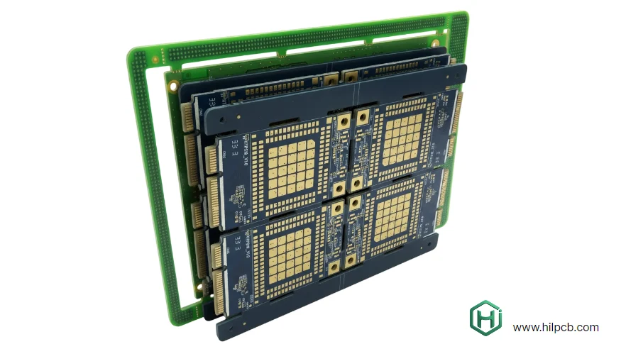
As AI and high-performance computing (HPC) surge globally, compute demand is growing exponentially. To push beyond the physical limits of Moore’s Law, the industry has shifted toward advanced packaging. Among these, TSMC’s CoWoS (Chip-on-Wafer-on-Substrate) has become a preferred solution for connecting high-performance logic (SoC) with high-bandwidth memory (HBM). However, the core foundation of this complex system—the CoWoS carrier substrate prototype—brings unprecedented design and manufacturing challenges. It is not “just a board”; it is a microscopic high-speed highway carrying trillion-level operations, and its performance can decide the success or failure of the AI chip.
From the perspective of an AI packaging and interconnect engineer, this article breaks down the key technical barriers behind a successful CoWoS carrier substrate prototype, covering Signal Integrity (SI), Power Integrity (PI), thermal management, material selection, manufacturing processes, and reliability validation. Whether you are an AI chip designer, system architect, or hardware engineer, understanding these challenges—and choosing the right manufacturing partner—is a decisive step in turning innovation into reality.
What exactly is a CoWoS carrier substrate prototype?
Before diving into technical details, we need a clear definition and its role in an AI chip system. Unlike a traditional PCB, a CoWoS carrier substrate is a high-density organic interposer layer whose complexity far exceeds a typical IC Substrate PCB. Positioned between the silicon Interposer and the final system motherboard, it serves two primary functions:
- Redistribution: Micro-bumps on the silicon interposer are spaced at micron-level pitch and cannot connect directly to a PCB. Through multiple fine routing layers (RDL) inside the substrate, the carrier “fans out” these high-density signals to a larger-pitch BGA so they can interface with the outside world.
- Power delivery and mechanical support: The carrier provides stable, low-noise power to the SoC and HBM dies above, and offers robust mechanical support to protect expensive silicon from stress damage.
A typical CoWoS carrier substrate prototype often uses low-loss materials such as ABF (Ajinomoto Build-up Film), includes dozens of routing layers, and reaches micron-level line width/space. For data-center deployments, the stability and performance of a data-center CoWoS carrier substrate are mission critical.
How do you ensure Signal Integrity for trillions of bits of data flow?
In a CoWoS architecture, HBM3/3e and the SoC connect through thousands of parallel data lines, reaching several Tb/s of bandwidth. At these frequencies, tiny physical defects can distort signals and trigger catastrophic data errors. Therefore, for a qualified high-speed CoWoS carrier substrate, Signal Integrity (SI) is the first priority.
Key control points include:
- Impedance Control: The impedance of signal paths must be held tightly around target values (e.g., 50 Ω) within very small tolerances. This requires precise control of Dk, dielectric thickness, copper thickness, and line width during fabrication. CoWoS carrier substrate impedance control is the foundation of high-speed transmission—any deviation causes reflections and eye degradation.
- Crosstalk: Dense routing makes EM coupling between adjacent lines unavoidable. You must optimize spacing, add ground shields, and plan routing layers to keep crosstalk within limits.
- Insertion Loss: Signals attenuate due to dielectric and conductor loss. Choosing ultra-low-loss substrate materials (e.g., ABF) is key. Optimizing Via structures—such as removing excess stub via back-drilling—can significantly improve high-frequency performance.
- Timing & Skew: For parallel buses like HBM, propagation delays must be highly consistent across all lines. Strict length matching and accounting for layer-dependent velocity are required to ensure synchronous arrival.
As an experienced PCB/substrate manufacturer, Highleap PCB Factory (HILPCB) uses advanced SI/PI co-simulation when supporting high-speed PCB designs, ensuring every step from design to manufacturing meets stringent high-speed performance requirements.
High-speed substrate material performance comparison
| Metric | Standard FR-4 | Mid-loss material | Ultra-low-loss (ABF-like) |
|---|---|---|---|
| Dielectric constant (Dk @ 10GHz) | ~4.5 | ~3.8 | ~3.2 |
| Loss factor (Df @ 10GHz) | ~0.020 | ~0.008 | <0.004 |
| Highest practical frequency | < 5 GHz | 5 - 15 GHz | > 25 GHz |
| Cost index | 1x | 2x - 4x | 5x - 10x+ |
Choosing the right material is the first step toward a high-performance high-speed CoWoS carrier substrate.
How do you build a stable PDN for hundreds of watts of AI silicon?
Modern AI chips can consume hundreds of watts, and their current demand can swing violently and rapidly. A poorly designed PDN can cause voltage droop (IR Drop), leading to functional errors or even system crashes. PDN design is therefore another core challenge for the CoWoS carrier substrate prototype.
Key PDN optimization strategies:
- Low-impedance paths: Use multiple dedicated power and ground planes inside the substrate to form wide, continuous low-impedance current loops. Thicker copper in critical areas reduces DC resistance.
- Decoupling capacitor network: Place a carefully planned network of decoupling capacitors to cover low-to-high frequency ranges. These capacitors act like micro energy reservoirs that respond quickly to transient current demands and stabilize supply voltage.
- Package–substrate co-design: PDN cannot be optimized in isolation. Co-simulate the chip package, carrier substrate, and system motherboard as a whole to minimize impedance across the entire delivery path.
- Avoid power-noise coupling: Plan power and signal layers to avoid coupling power noise into high-speed nets—also critical for stable CoWoS carrier substrate impedance control.
What are the traps in stack-up design and material selection?
The CoWoS carrier stack-up is the blueprint that determines electrical performance, thermal behavior, and mechanical reliability. A small mistake can fail an entire prototype program.
Key points to watch:
- Symmetry: To control Warpage during manufacturing and assembly, the stack-up must be strictly symmetric—including dielectric thickness, copper thickness, and distribution. Warpage is a primary driver of CoWoS carrier substrate assembly yield.
- RDL and microvia technology: RDL is typically built with SAP or mSAP to achieve micron-scale features. Inter-layer connectivity relies on laser-drilled Microvias. Microvia reliability—especially stacked-via structures—is a core metric for CoWoS carrier substrate reliability.
- Material selection: ABF and other advanced low-CTE, low-Dk/Df materials are preferred. CTE must be matched to silicon to reduce thermo-mechanical mismatch stress—critical for long-term reliability.
- Reference-plane integrity: All high-speed nets must have continuous reference ground or power planes. Any split or discontinuity causes impedance jumps and reflections.
HILPCB has industry-leading HDI PCB and IC substrate manufacturing capability, enabling complex stack-ups and precision microvia processes to provide a solid manufacturing foundation for your CoWoS substrate prototype.
🔬 HILPCB advanced packaging: core capabilities for CoWoS carrier substrate prototyping
15 / 15 μm
supports ultra-high-density interconnect for HPC
50 μm
meets advanced HDI vertical interconnect needs
± 5%
for HBM3/PCIe 6.0 signal environments
< 50 μm
ensures success rate for large-size Die Bonding
20+ Layers
enables efficient power delivery for multi-die modules
ABF-like / LCP
a seamless Scale-up path from prototype to volume
Industry insight: In CoWoS carrier substrate manufacturing, RDL feature size directly impacts communication bandwidth between logic silicon and HBM. By introducing semiconductor-like process control, HILPCB holds RDL line width at 15μm and combines it with excellent warpage management—effectively mitigating thermo-stress mismatch issues in 2.5D/3D packaging.
How do you manage the massive heat of AI silicon effectively?
Cooling is the lifeline for stable AI operation. An AI accelerator at 700W or even 1000W can have extremely high heat flux density. If heat is not removed quickly and effectively, the chip will throttle or suffer permanent damage. In the overall heat path, the CoWoS carrier substrate plays a critical bridge role.
Effective thermal-management strategies include:
- Co-simulated thermal analysis: At design stage, run system-level thermal simulations across the chip, interposer, carrier substrate, heat spreader/sink, and TIM to accurately predict hotspot location and temperature distribution.
- Optimize conductive paths inside the substrate: Use dense Thermal Vias and thicker copper planes to build efficient vertical and lateral conduction channels, quickly transferring heat to the substrate underside.
- Advanced cooling materials: Integrating a Vapor Chamber or using higher-thermal-conductivity TIM can significantly improve cooling. The thermal conductivity of the substrate material itself should also be considered.
- Data-center-oriented design: For data-center CoWoS carrier substrate, consider the server rack airflow and liquid-cooling system to align substrate design with system-level cooling solutions.
From design to manufacturing: how do you cross the DFM gap?
Even a theoretically perfect CoWoS carrier substrate prototype is meaningless if it cannot be manufactured economically and reliably. Design for Manufacturability (DFM) is the bridge between design intent and physical reality.
Core DFM considerations:
- Match process capability: Designers must understand the manufacturer’s limits (minimum line width/space, minimum drill size, lamination registration, etc.) and keep adequate margins.
- Panelization: Multiple substrate units are combined on a large production panel for efficiency. Good panelization maximizes material utilization and helps control stress distribution to reduce warpage.
- Test point design: Reserve sufficient test points to enable electrical test (e.g., flying probe) and verify all net connectivity.
- Early communication with the manufacturer: Engage a manufacturer like HILPCB early and follow DFM guidelines to avoid late-stage redesign, saving time and cost. HILPCB provides free DFM checks to help customers detect and correct potential manufacturing risks before release.
🛡️ HILPCB end-to-end flow for CoWoS carrier substrate prototypes
Complete multi-physics co-analysis across SI/PI/Thermal. Define the substrate stack-up to optimize both high-speed signal paths and thermal spreading paths.
Submit design files to the HILPCB expert bench. We pre-review and optimize etch compensation for 15μm features, ABF lamination stress, and manufacturing feasibility.
Use modified semi-additive process (mSAP). With vacuum lamination and precision pulse plating, achieve reliable fill and interconnect for high aspect-ratio Micro-via.
Integrate AOI, 3D-Xray, and 100% warpage testing. Ensure every prototype meets impedance tolerances and provide a complete Verification Report.
“A four-in-one closed loop that ensures accurate translation from design to physical prototype.”
How do you ensure long-term reliability under harsh conditions?
An AI accelerator module can have a lifecycle of many years, experiencing countless power on/off thermal cycles and sustained high-temperature operation. CoWoS carrier substrate reliability is the bedrock for long-term stable operation.
Reliability validation typically follows industry standards such as IPC and JEDEC and includes harsh environmental stress tests:
- Temperature cycling test (TCT): Simulates repeated changes between extreme temperatures (e.g., -40°C to 125°C) to evaluate whether thermo-expansion mismatch stress causes microvia cracking or solder-joint failure.
- Highly accelerated stress test (HAST): Accelerates material aging under high temperature, humidity, and pressure to assess moisture resistance and long-term chemical stability.
- Mechanical shock and vibration: Simulates physical impacts during transport and operation to verify structural strength and solder-joint mechanical reliability.
These tests expose potential weaknesses in design and manufacturing, enabling continuous improvement toward truly robust products.
CoWoS carrier substrate assembly: the last critical kilometer
After carrier fabrication, CoWoS carrier substrate assembly is the last step to integrate it with silicon into a functional module—and one of the most technically demanding steps.
Key assembly steps and challenges:
- BGA ball attach: Precisely attach thousands of solder balls on the underside for connection to the system motherboard. Ball height and coplanarity must be tightly controlled.
- Interposer and die attach: Use high-precision Flip-Chip equipment to place the silicon interposer, SoC, and HBM onto the carrier. Alignment accuracy is micron-level.
- Reflow: Solder with tightly controlled thermal profiles. Poor profiles can cause defects or thermal damage to silicon. Substrate warpage is most influential at this stage.
- Underfill: Dispense and cure epoxy underfill between die and carrier to spread thermo-mechanical stress, protect micro joints, and dramatically improve reliability.
- Final test and inspection: Use X-Ray to inspect internal joint quality and run functional tests to validate electrical performance.
Beyond top-tier substrate manufacturing, HILPCB also provides one-stop SMT Assembly and Prototype Assembly through partner networks—delivering turnkey services from bare boards to complete SiP (System-in-Package) modules and simplifying supply-chain management.
Conclusion: choose the right partner and master complexity
Building a successful CoWoS carrier substrate prototype is a complex systems engineering effort that requires a delicate balance across SI, PI, thermal management, materials science, and precision manufacturing. From the initial design concept to the final functional module, every step is challenging—and any weak link can delay or even derail the program.
In an era of rapid iteration, partnering with an experienced, technically leading, and highly responsive manufacturer matters more than ever. With deep expertise in IC substrates and high-density interconnect, advanced manufacturing capability, and a strong commitment to quality, HILPCB is dedicated to helping AI innovators turn frontier designs into reality. We understand the pressure and challenges you face in developing a CoWoS carrier substrate prototype, and we are ready to be your most trusted partner—with engineering depth and one-stop services.
Contact HILPCB today to launch your next-generation AI substrate interconnect project—and let’s push the future of AI forward together.