
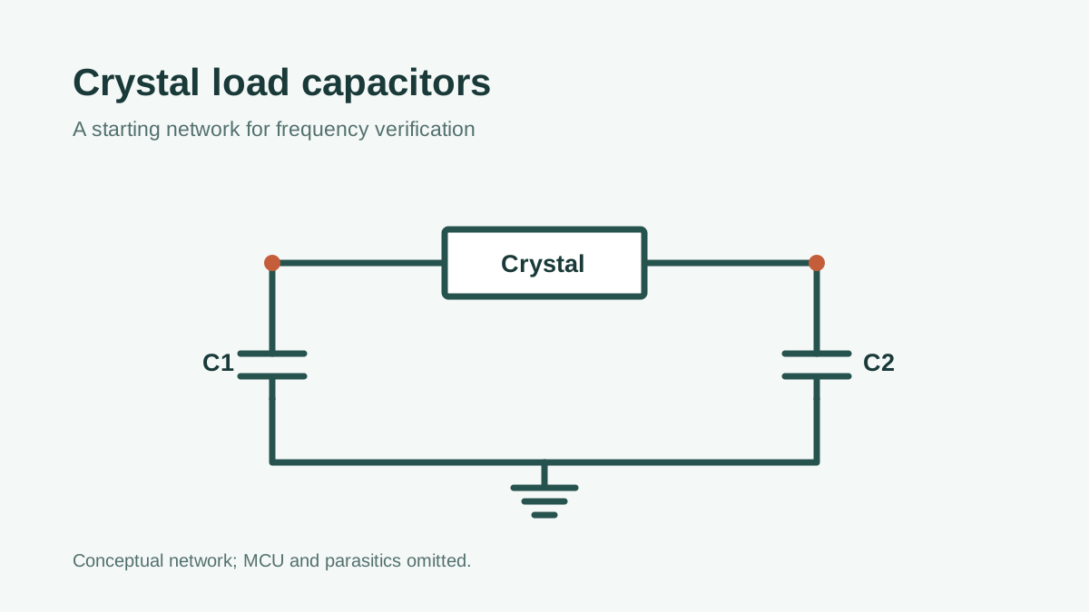
Start with the load capacitance specified for the exact parallel-resonant crystal, then choose a capacitance model that accounts for the exact MCU oscillator mode and board. Under the lumped-parasitic model defined below, an initial equal-capacitor pair is:
C1 = C2 = 2 × (CL - Cs)
This is a starting calculation, not a qualification result. Verify frequency on assembled hardware with a sufficiently low-loading or buffered measurement method. Then check startup margin and crystal drive separately, using the applicable MCU and crystal documentation.
1. Define the parts and the capacitance model
Before calculating, record:
- The MCU’s full orderable part number, oscillator pins and selected operating mode.
- The crystal’s full orderable part number, nominal frequency and specified load capacitance,
CL. - The crystal’s relevant tolerance, temperature, equivalent series resistance (ESR) and maximum drive specifications.
- The MCU’s internal pin capacitance and any fixed or programmable oscillator load capacitance applicable to that mode.
- The intended capacitor tolerances and a documented estimate or measurement basis for board parasitics.
The crystal’s specified CL is the load for which its nominal frequency is specified. It is not automatically the value of each external capacitor. Microchip AN826 / DS00826A discusses the specified crystal load and external Pierce network for its covered rfPIC and PICmicro devices. For a particular design, the exact crystal and MCU documents take precedence.
The explicitly lumped model
For this calculation, define:
C1: the first external capacitor from an oscillator node to the circuit’s reference.C2: the second external capacitor from the other oscillator node to the reference.Cs: a single effective lumped correction for all relevant parasitic and internal capacitance contributions not already represented inC1andC2, according to this model.CL: the resulting effective load presented to the crystal.
The model is:
CL = (C1 × C2) / (C1 + C2) + Cs
This simplified form expresses the two external capacitors as a series equivalent with a separate effective correction. Microchip AN826 / DS00826A presents a lumped stray-capacitance form for its covered devices; use the selected MCU's guidance to determine which contributions belong in the correction.
The important word is effective. In this convention, Cs is not necessarily the simple sum of every capacitance on both pins. It represents their combined effect in the stated equation. Its value depends on the model and the actual circuit; it is not a universal PCB allowance.
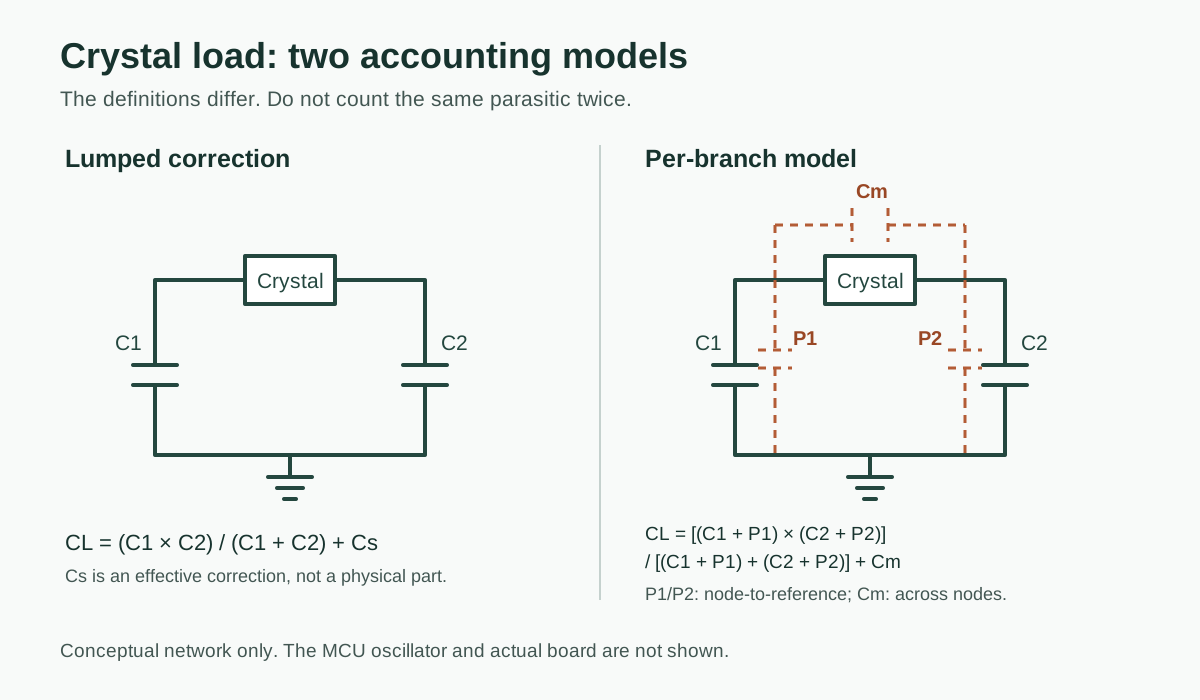
The drawings show capacitance accounting only; the MCU oscillator and real board are omitted.
Equal external capacitors
If the chosen model and MCU documentation permit equal external capacitors, set C1 = C2 = C:
CL = C/2 + Cs
Rearranging gives:
C = 2 × (CL - Cs)
If CL - Cs is zero or negative, this equation does not produce a positive external-capacitor pair. Recheck the model, the internal-capacitance setting and the input values. Do not force a capacitor selection without consulting the applicable device and crystal guidance.
Equal capacitors simplify the arithmetic; they are not a requirement for every oscillator. If the MCU documentation specifies unequal values, an internal network, or a different method, use that guidance instead.
| Input or condition | Decision before choosing capacitors | If unresolved |
|---|---|---|
| Exact crystal and specified load | Use the load and limits for the orderable part and operating conditions | Hold the calculation until the part documentation is available |
| MCU oscillator mode and internal network | Follow the device-specific mode and account for each contribution once | Resolve the configuration and its capacitance convention |
| Parasitic model and board estimate | Define lumped or branch terms, their assumptions and any measurement basis | Treat the result as an unverified starting point |
| External capacitor tolerance and available values | Compare candidate parts and tolerances with the product's frequency budget | Do not assume the nominal calculated value is a qualified selection |
| Frequency, startup and drive evidence | Define separate checks for the assembled circuit and relevant conditions | Keep release conditional until the product authority reviews evidence |
2. Work through a hypothetical initial calculation
The following numbers are invented solely to show the arithmetic. They do not describe a real MCU, crystal, PCB or expected frequency performance.
Assume:
- The hypothetical crystal specifies
CL = 12 pF. - The effective lumped correction is exactly
Cs = 2 pF, including all modeled internal and board contributions. - The MCU has no additional enabled programmable load bank outside that correction.
- Both external capacitors are identical and exact.
For arithmetic only, assume the correction stays fixed and ignore tolerance, temperature and frequency dependence and active oscillator behavior.
Then:
C1 = C2 = 2 × (12 - 2) = 20 pF
The model check is:
CL = (20 × 20) / (20 + 20) + 2 = 10 + 2 = 12 pF
Thus, 20 pF per branch is an initial nominal pair only under these hypothetical assumptions. Account for actual component tolerances and test the assembled circuit before release.
3. Do not mix lumped and per-branch parasitics
A different model assigns parasitics to the two branches rather than collecting their effects in one Cs. For example, define P1 and P2 as the relevant added capacitances from each oscillator node to reference, and Cm as a separately modeled capacitance directly between the two crystal nodes:
CL = [(C1 + P1) × (C2 + P2)] / [(C1 + P1) + (C2 + P2)] + Cm
This is a different bookkeeping convention. Adding P1 + P2 directly as though it were the lumped Cs generally gives the wrong result. For the symmetric case C1 = C2 = C and P1 = P2 = P, the equation reduces to:
CL = C/2 + P/2 + Cm
With fixed P and Cm, the effective lumped correction is P/2 + Cm and does not depend on C. Asymmetric branches or parasitics that change with value can produce different behavior.
TI's MSP430 32-kHz Crystal Oscillators, SLAA322D, revised July 2017, discusses MCU and PCB capacitance per branch in section 2.1. Its symmetric example uses a 12 pF load and 2 pF parasitic per pin, giving 22 pF on each branch. The hypothetical example above instead uses a 2 pF effective lumped correction, giving 20 pF. TI's device settings and tests are not universal guidance for every MCU or MHz oscillator.
Exact-part candidate example: MSP430FR2355TPT and ECS-.327-12.5-12-TR
This is a documented candidate pair and a hypothetical calculation, not a compatibility or qualification result.
The TI MSP430FR235x / MSP430FR215x data sheet, SLASEC4D, revised December 2019, identifies the MSP430FR2355TPT as a 48-pin LQFP device. Its pin diagram identifies pin 8 as XIN and pin 9 as XOUT. The ECS ECX-12 data sheet, Rev. 2017, identifies ECS-.327-12.5-12-TR as a 32.768 kHz crystal with a 12.5 pF specified load.
For crystal operation, the TI data sheet distinguishes LFXTBYPASS = 0 from the logic-level clock-input mode. The data sheet and the MSP430FR4xx and MSP430FR2xx Family User's Guide, SLAU445I, revised March 2019, call for external capacitors at both crystal terminals. The guide also says the shared pins default to GPIO and must be configured for oscillator operation.
For arithmetic only, assume equal branches, 2 pF total parasitic per branch including MCU-pin and PCB contributions, and zero cross-node contribution:
12.5 pF = (Cext + 2 pF) / 2
Cext = 23 pF on each branch
Check: (23 pF + 2 pF) / 2 = 12.5 pF.
The 23 pF result is an ideal model result, not a qualified capacitor selection. The assumed 2 pF total per branch is not a measurement of a PCB. TI lists approximately 2 pF per pin for bond and package parasitics, and actual PCB capacitance adds to that contribution. The total can therefore differ from the assumption. Account for asymmetry and cross-node capacitance without double counting; do not add the data sheet’s integrated effective load value again without understanding what it includes.
The ECS data sheet lists a maximum ESR of 90 kΩ, typical drive of 0.1 µW and maximum drive of 0.5 µW. These specifications and the calculation do not establish compatibility, startup margin, acceptable drive or frequency performance for the pair. Before using it, check current manufacturer documents and validate the actual circuit, including frequency, startup or negative-resistance margin, and drive over the relevant conditions.
Account for internal capacitance once
Some MCUs have oscillator-pin capacitance, internal load capacitors, programmable load settings, or a combination. Determine what each published value means for the selected mode:
- Identify which internal capacitances are present or enabled.
- Determine whether the MCU’s recommended external values already account for them.
- Put each contribution in one place in the chosen model: within the lumped effective correction, within a defined branch, or as instructed by the MCU’s own calculation.
- Do not add the same internal capacitance again as PCB stray or as another external-equivalent allowance.
If the documentation does not make the accounting clear, resolve that question before treating the calculated pair as a design decision. A neat equation cannot compensate for an undefined input.
4. Verify frequency without making the probe part of the load
Build the candidate circuit on an assembly representative of the intended product. Configure the oscillator and firmware as intended, and use the measurement method recommended for that exact device wherever possible.
A buffered clock output can be preferable when the MCU provides an appropriate one. Confirm what signal it exposes and whether a divider or other clock configuration must be accounted for. The buffer output measurement should not be assumed to equal the crystal frequency until that relationship is established.
If measurement at a crystal node is necessary, assess the probe’s capacitance and other loading effects as part of the measurement. A connection that changes the effective load can change the result or disturb oscillation. TI SLAA322D specifically warns about probing effects in its documented low-frequency oscillator context; the suitable method for another design must be established from its own documentation and measurement setup.
Record at least:
- Board revision, MCU and crystal orderable parts, capacitor values and tolerances.
- Internal load configuration and firmware or register settings.
- Measurement point, instrument, probe or buffer arrangement, and any divider.
- Supply and temperature during the measurement.
- Frequency reference, instrument uncertainty and measurement duration.
- Measured frequency and the applicable frequency requirement.
For a nominal frequency f_nominal, express a measured deviation as:
Frequency deviation in ppm = [(f_measured - f_nominal) / f_nominal] × 1,000,000
Compare that result with the complete product frequency budget, not just with zero error. Crystal initial tolerance, temperature behavior, measurement uncertainty and other applicable contributors must be considered.
A frequency measurement can indicate whether the assembled circuit is meeting its frequency requirement under the measured conditions. It does not, by itself, identify the exact effective capacitance or prove that the oscillator will start reliably, remain within drive limits, or meet the requirement under every condition.
5. Check startup and drive as separate decisions
Startup and loss margin
An oscillator can run on one bench sample yet have insufficient margin when components, supply or environment vary. Use the startup or oscillator-margin method specified for the exact MCU and crystal, including the relevant crystal ESR and operating conditions.
The applicable documentation may describe a negative-resistance or other margin evaluation. Use its procedure and acceptance criteria only where they apply; do not transfer a numerical margin from TI SLAA322D to an unrelated oscillator.
Also test startup behavior under the product’s relevant conditions and sequences. The required combinations and pass criteria belong in the product’s verification plan.
Crystal drive level
Check drive against the maximum drive specification for the exact crystal, using a measurement or calculation method appropriate to the oscillator and documented by the relevant manufacturers. Excess drive and inadequate startup margin are different risks; passing one check does not establish the other.
Microchip AN826 discusses excessive drive as a separate concern for its covered products. Its age and device scope make current documentation for the selected parts especially important.
Changes made to address drive or startup can affect the oscillator. After an approved change, repeat the relevant frequency, startup and drive checks rather than assuming the original results still apply.
6. Validate a production-representative design
The calculation selects a candidate; validation establishes whether the intended design meets its requirements. Use representative:
- PCB layout and stackup, assembly process, cleaning and handling.
- MCU, crystal and capacitor parts, including relevant tolerances and variations.
- Supply conditions, operating temperatures and environmental exposure.
- Firmware configuration, startup sequences and clock-output configuration.
Define the sample plan, operating-condition coverage and acceptance criteria before interpreting results. Record failures and retest decisions as well as passes. In particular, a successful room-temperature frequency reading on one prototype is not evidence for all production units or conditions.
Layout choices affect parasitics and susceptibility to disturbance, but no single spacing, guard, ground arrangement or stray-capacitance number is appropriate for every oscillator. Follow the exact device and crystal guidance, then validate the actual board.
Design and handoff checklist
Before releasing the design package, make sure it includes:
- Exact MCU and crystal orderable part numbers and applicable document revisions.
- Oscillator mode, firmware settings and internal-capacitance configuration.
- Crystal
CL, tolerance, ESR and maximum drive requirements. - External capacitor part numbers, nominal values and tolerances.
- The chosen capacitance model, definitions and assumptions, with no double counting.
- Calculation and rationale for the initial capacitor pair.
- Frequency measurement method, loading assessment, uncertainty and results.
- Separate startup-margin and drive-level procedures, criteria and results.
- Production-representative validation plan, coverage, results and open issues.
- Approved PCB, assembly and test documentation for the revision being handed off.
For PCB assembly, provide the approved BOM, component and placement files, oscillator configuration and relevant assembly requirements. An assembly inspection report can document the agreed inspection scope and results. When you request a quote, agree on any required testing separately: a quote or routine assembly inspection is not evidence of oscillator frequency, startup margin or crystal drive qualification.
FAQ
Is each load capacitor equal to the crystal’s specified load capacitance?
Not generally. In the defined lumped model, the two external capacitors contribute through their series equivalent, plus the effective parasitic correction. For equal capacitors, the initial value of each is 2 × (CL - Cs).
What value should I use for stray capacitance?
Use a value or model justified for the exact MCU, layout and accounting convention. There is no universal value. Be clear whether internal pin and programmable capacitances are included, and do not count them twice.
Can I use the same capacitor calculation for internal load banks?
Only if the model accurately represents the enabled internal network and the MCU documentation permits that interpretation. Some devices specify settings or calculation methods that should be followed directly.
Does an accurate frequency reading prove the oscillator is robust?
No. It shows frequency performance for the measured assembly and conditions, subject to measurement uncertainty. Startup margin, crystal drive and performance across the required operating and production conditions need separate checks.
What if probing changes the oscillator frequency?
Treat the reading as potentially loaded. Prefer a suitable buffered output or the exact device manufacturer’s recommended method. If a crystal node must be probed, include the probe’s loading in the analysis and document the setup.