
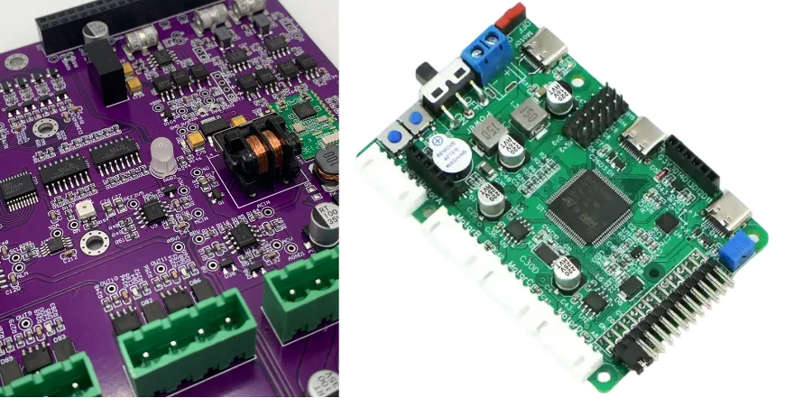
As a power drive engineer focused on IGBT/GaN drive and regenerative energy handling, I know that in modern automation systems, control boards are the nervous system connecting digital commands to physical actuation. In data centers—where reliability, efficiency, and real-time behavior are held to an extreme standard—the design and manufacturing of data-center PROFINET control PCB face unprecedented challenges. It must meet nanosecond-level synchronization demands introduced by the PROFINET industrial Ethernet protocol, while also driving high-power IGBT or high-speed GaN devices precisely and reliably, and remaining stable under harsh EMI conditions. From a power-drive perspective, this article breaks down the core technical points behind a high-performance data-center PROFINET control PCB, including gate drive, multi-layer protection, passive placement strategy, and EMC compliance.
PROFINET real-time requirements for power-drive control PCB
As a leading industrial Ethernet standard, PROFINET’s key advantage is deterministic real-time communication. In its IRT (Isochronous Real-Time) mode, cycle times can be as low as 31.25μs with jitter under 1μs. This level of determinism places extremely high demands on the power-drive control loop. In data-center robotics (e.g., automated tape libraries, server-handling robots), communication delay or jitter can translate into torque ripple or positioning error—directly impacting performance and reliability.
Therefore, the data-center PROFINET control PCB must tightly couple communication real-time behavior with power-drive transient response. That means:
- Low-latency processing: from receiving a PROFINET frame to updating PWM outputs, the end-to-end path must be controlled within microseconds.
- Clock synchronization: the on-board MCU or FPGA must synchronize precisely to the PROFINET network clock to ensure coordinated multi-axis motion.
- Noise immunity: high-speed switching in the power stage generates strong EMI. Layout and shielding must prevent interference with the PROFINET PHY and communication traces, ensuring data integrity.
Achieving strict PROFINET control PCB compliance is not only a software/protocol problem—it is the ultimate test of hardware design and PCB physical implementation.
IGBT/GaN gate-drive design: suppress Miller effect and common-mode interference
The gate-drive circuit is the “heart” of the power device. Its performance directly determines switching loss, EMI level, and system reliability. When designing the drive stage for data-center PROFINET control PCB, focus on:
Miller-effect suppression
Miller capacitance (Cgc) creates the Miller plateau during switching, increasing transition time and loss. More dangerously, in bridge topologies, when one device turns on quickly, the fast dV/dt can drive displacement current through the Cgc of the opposing off device, unintentionally “inducing” turn-on and causing shoot-through.
Solutions:
- Negative turn-off: provide a negative gate-off voltage (e.g., -5V to -9V) to increase noise margin and prevent Miller turn-on.
- Active Miller clamp: during turn-off, when Vgs drops below a threshold, the driver provides a very low-impedance clamp path to GND or negative rail, giving Miller current a bypass and preventing gate voltage rise.
- Asymmetric Gate Resistor: use a small Rg_on for fast turn-on and a larger Rg_off to suppress turn-off ringing and dV/dt. This is often implemented with a diode in parallel with a resistor.
Drive-loop minimization
Parasitic inductance in the gate-drive loop (driver output → gate resistor → gate → source/emitter → driver ground) is the #1 performance killer. It causes severe gate ringing, can exceed device Vgs_max, and generates strong EMI. During PROFINET control PCB assembly, placement is extremely demanding: put the driver as close as possible to the power device, use wide/short traces, and even use stack-up techniques to minimize loop area.
Key reminder: core tradeoffs in drive design
- Speed vs. reliability: very fast switching (low Rg) reduces switching loss but worsens overshoot and EMI. You must balance efficiency and EMC.
- Drive power quality: the isolated DC/DC powering the gate driver must have low parasitic capacitance and high CMTI to stay stable under high dV/dt.
- GaN drive specifics: GaN HEMT has a narrower Vgs window and lower threshold voltage, making it more sensitive to drive-loop inductance. Specialized GaN drivers and more aggressive layout are often needed, such as integrating the driver and GaN device into the same package (DrGaN) or using [multilayer PCB](/products/multilayer-pcb) to place the drive loop on adjacent layers.
DESAT protection and short-circuit response: ensuring system-level safety
In data centers, any downtime can be extremely costly. Therefore, short-circuit protection in the power stage is critical. DESAT (desaturation) protection is one of the most common and reliable short-circuit protection mechanisms for IGBT.
Working principle: When the IGBT is on normally, Vce(sat) is low (typically 1–3V). In a short circuit, current rises sharply, the IGBT leaves saturation, and Vce rises quickly. The DESAT circuit monitors Vce via a high-speed diode; if it exceeds a threshold (typically 7–9V), protection triggers.
Key design points:
- Blanking Time: at turn-on, Vce needs time to drop from high voltage to Vce(sat). DESAT must be blanked to avoid false trips. This is typically 1–2μs and must be controlled precisely.
- Soft turn-off: when a short is detected, you cannot hard turn-off instantly. With huge bus current, fast turn-off creates lethal voltage spikes on stray inductance (L * di/dt). Use a high-impedance path to pull down the gate slowly and control di/dt.
- Fault feedback: after protection triggers, the driver should immediately signal the MCU. The MCU then reports status via PROFINET to higher-level monitoring for system-level diagnostics and handling—essential to overall PROFINET control PCB quality.
For complex PROFINET control PCB programs, iterative validation through prototype assembly is often necessary to tune DESAT and other protection parameters.
Snubber networks and buffer circuits: managing dV/dt and voltage overshoot
During turn-off, parasitic inductance (Lσ) in the power loop resonates with the device output capacitance (Coss), causing serious overshoot and ringing. This threatens avalanche breakdown voltage (Vbr) and becomes a major EMI radiation source. The purpose of a Snubber network is to suppress this resonance.
RC/RCD snubbers
- RC Snubber: a series resistor + capacitor across the device, providing a damping path for high-frequency resonant current and dissipating energy as heat in the resistor.
- RCD Snubber: adds a diode to RC, mainly for voltage clamping. During turn-off, inductive energy charges the capacitor through the diode and clamps voltage to a level.
Layout is the key: Snubber effectiveness is 90% layout. The Snubber loop (device drain/collector → Snubber C/R → device source/emitter) must be the smallest loop in the power stage. Any extra trace length adds inductance and destroys effectiveness. In data-center PROFINET control PCB design, we often use heavy copper PCB for high current, while carefully placing Snubber components right next to device pins. This consistency is critical for PROFINET control PCB mass production because small placement differences can cause large performance variation.
Assembly advantage: precision soldering and component placement
For power-drive boards—especially PCBs containing key loops like Snubber and gate drive—assembly quality directly impacts final performance. Professional PROFINET control PCB assembly helps ensure:
- Tight component placement: minimize distances between power devices, drivers, and passives to reduce parasitics.
- Soldering consistency: use reflow or wave soldering to ensure low resistance and high reliability of all joints—especially on power paths—to avoid local overheating.
- Thermal integration: precisely install heatsinks, thermal pads, and related parts so device heat is removed efficiently—critical to overall PROFINET control PCB quality and long-term reliability.
High-accuracy current sensing: layout considerations for shunt and Hall sensors
Accurate current measurement is the foundation for high-performance closed-loop control (e.g., FOC) and overcurrent protection. Common methods include Shunt resistors and Hall-effect sensors.
Shunt resistor
A Shunt is a very low-value (mΩ-level) precision resistor.
- Pros: good linearity, low drift, wide bandwidth, low cost.
- Challenges:
- Parasitic inductance: even “non-inductive” shunts still have small parasitic inductance that can create spikes under high-frequency switching current.
- Kelvin Connection: accurate measurement requires 4-wire Kelvin connection. Sense traces must route from the inner side of the shunt pads to avoid voltage drop on solder joints caused by the high-current path.
- Signal conditioning: shunt voltage is tiny (tens of mV) and rides on a high common-mode voltage. Use differential or isolated amplifiers with high CMRR.
Hall-effect sensor
- Pros: inherent isolation, convenient for large current.
- Challenges: higher cost, zero drift, relatively limited bandwidth.
In data-center PROFINET control PCB layout, current-sense routing is a top SI priority: these weak analog signals are easily corrupted by switching noise. Route them as differential pairs, keep away from high dV/dt and dI/dt regions, and shield with ground planes.
Isolation and EMC design: dealing with high dV/dt and PROFINET compliance
Finally, isolation and EMC are equally critical. data-center PROFINET control PCB must build a strong barrier between two worlds: a noisy, high-voltage, high-current power world, and a sensitive low-voltage digital control/communication world.
Electrical isolation
- Functional isolation: ensures control circuitry operates correctly.
- Basic/reinforced insulation: meets safety requirements to protect people and equipment.
- Implementation: digital isolators (capacitive or magnetic), optocouplers, and isolated power modules.
In PCB terms, isolation means strict physical separation. HV and LV grounds must be fully separated, with defined Creepage and Clearance between them. Any trace crossing the isolation barrier must go through designated isolation components.
EMC design
EMC is key to PROFINET control PCB compliance. PROFINET specifies immunity and emissions requirements.
- Control radiation at the source:
- Minimize loop area: the golden rule. Reducing high-frequency current loops (power loop, gate-drive loop) significantly reduces differential-mode radiation.
- Control dV/dt and dI/dt: adjust gate resistors, add soft-switching circuits, and slow switching appropriately while meeting performance.
- Block conducted paths:
- Common-mode choke (CMC): use CMCs at power inputs and PROFINET cable interfaces to suppress common-mode noise.
- Y capacitors: connect Y caps between HV and LV grounds to provide a low-impedance return path for common-mode current; choose capacitance and voltage rating carefully per leakage current and safety requirements.
- Grounding and shielding:
- Unified LV ground plane: provide stable reference for PROFINET controller, PHY, and digital logic.
- Shielding: locally shield sensitive analog circuits (e.g., current sense) and PROFINET communication lines.
For complex EMC problems, using impedance calculators and similar tools to precisely control key transmission-line impedance is an effective way to maintain both signal quality and EMC performance.
Conclusion
Designing a successful data-center PROFINET control PCB is complex systems engineering. Engineers must master not only PROFINET protocols, but also the deeper principles of power electronics. From nanosecond-level gate-drive control, to microsecond-level short-circuit protection response, to millisecond-level control-loop regulation—every time scale is built on solid PCB physical design.
Miller effect, parasitic inductance, thermal management, SI, and EMC must be considered as a whole from the first design stage. This determines not only board-level performance but also the reliability, safety, and long-run economics of the entire automation system. Ultimately, achieving high-quality PROFINET control PCB mass production requires full-stack control from design and simulation to precision manufacturing and strict testing. Only then can we master real-time performance and safety redundancy, and build a powerful core for stable future data-center automation.