
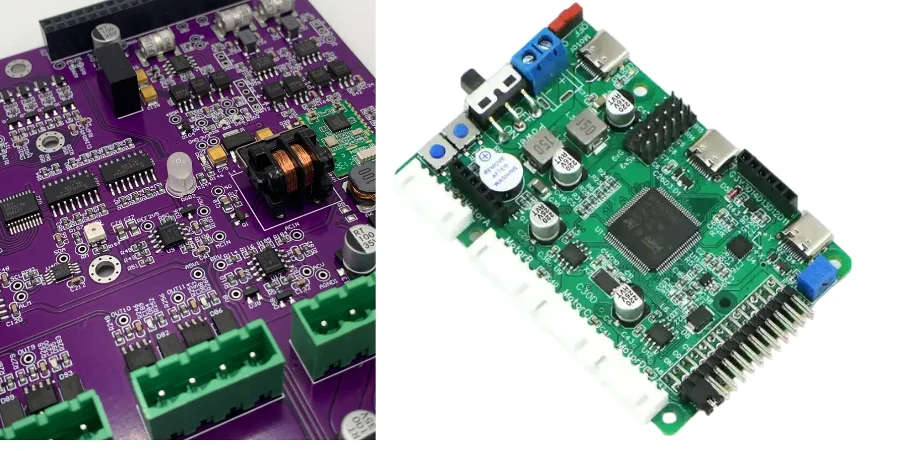
In the Industry 4.0 era, industrial robots and automation systems sit at the center of smart manufacturing. The “nervous system” of these controllers—the PCB—must carry real-time communications, precision motion control, and functional safety. For high-speed real-time industrial networks such as EtherCAT, PROFINET, and CANopen, PCB design and manufacturing face unprecedented constraints. Even small design flaws or process deviations can trigger latency, data errors, or system downtime. That’s why a thorough DFM/DFT/DFA review is essential to deliver performance, reliability, and cost efficiency. From the perspective of an industrial network engineer, this article explains how a systematic DFM/DFT/DFA review helps you control real-time behavior, safety redundancy, and EMC—especially for demanding industrial interface boards and high-speed Servo motor driver PCB programs.
The core of DFM/DFT/DFA review: beyond a traditional manufacturability check
Traditional PCB reviews often focus on functional correctness and underweight manufacturability, testability, and assembly. In complex industrial control, that siloed approach is risky. A complete DFM/DFT/DFA review merges the three dimensions into a closed-loop optimization flow that protects the full product lifecycle.
- DFM (Design for Manufacturability): the foundation. DFM asks whether the PCB can be fabricated stably with high yield and controlled cost. It covers minimum line/space, drilling accuracy, stackup structure, impedance tolerances, copper thickness uniformity, and more. For example, when building a high-speed PCB, a DFM review will scrutinize differential length matching, reference-plane continuity, and via selection (e.g., blind/buried vias) to keep SI intact through fabrication.
- DFT (Design for Testability): quality control. DFT ensures the PCB can be tested efficiently and thoroughly after manufacturing. Key items include critical Test Point placement, JTAG/Boundary Scan access, and ICT probe accessibility. For safety-critical programs like
Dual-channel safety control PCB mass production, DFT is especially important: each safety channel’s critical nodes must be verified independently and reliably to support SIL (Safety Integrity Level) certification. - DFA (Design for Assembly): production efficiency and product reliability. DFA focuses on placement, soldering, and final assembly constraints: component spacing, pad design, silkscreen clarity, connector orientation/accessibility, heatsink clearance, etc. Strong DFA reduces SMT defects (opens/bridges) and simplifies downstream system integration such as Box Build Assembly.
Together, they form the foundation for Servo motor driver PCB reliability.
EtherCAT/PROFINET clock synchronization and jitter control
Real-time Industrial Ethernet depends on precise time synchronization. EtherCAT Distributed Clocks (DC) and PROFINET time sync (PTP/IEEE 1588) require nanosecond-class timestamp accuracy. Any PCB weakness can introduce jitter and break the sync mechanism.
PCB challenges for clock synchronization:
- Clock-tree design: from the crystal to the PHY and up to the MAC controller, the clock path must be treated as a transmission-line system. Length, branching topology, and termination directly affect clock quality.
- Power noise: noise on the rails couples into the clock and creates phase jitter. A low-noise PDN with strong PSRR behavior is critical.
- Crosstalk: coupling between the clock and nearby high-speed data nets or switching-noise sources is a common jitter contributor.
Mitigations inside a DFM/DFT review:
- DFM: enforce impedance control and ensure clock differential-pair geometry (when used) is accurate—width, spacing, and distance to reference planes. In stackup planning, place the clock layer between solid GND planes (Stripline) for best shielding. For complex
PROFINET control PCB design, simulation should be used to validate the full clock-tree SI. - DFT: reserve high-frequency measurement access near key clock nodes (e.g., PHY clock input). These test points are often miniature coax connectors or dedicated probe pads, enabling production measurements of jitter and phase noise using oscilloscopes or time-interval analyzers so every board meets the protocol spec.
Physical-layer optimization: PHY + magnetics placement and signal integrity
The PHY and its magnetics are the “gateway” of an Industrial Ethernet interface. Placement and routing here directly determine communication quality and EMC.
Key placement rules:
- Shortest path: place the PHY as close as possible to the magnetics and the RJ45 connector to minimize the MDI differential path length.
- Symmetry: route Tx+/Tx- and Rx+/Rx- with strict symmetry—length, via count, and bend radius—to maintain differential impedance balance and suppress common-mode noise.
- Moat/isolation band: create a clear separation between the PHY analog side (to magnetics) and digital side (to MAC). Split the ground in the moat and connect through a single point (typically a 0Ω resistor or ferrite bead) to prevent digital noise from polluting the analog domain.
DFA considerations: During assembly, magnetics and RJ45 are often large THT parts. DFA must ensure:
- Process compatibility: if the PCB is reflow-centric SMT, can the THT parts be assembled via Pin‑in‑Paste, or is wave/selective soldering required? This affects cost and throughput.
- Mechanical stress: RJ45 experiences insertion/extraction forces. DFA reviews pad design and mounting features to prevent long-term solder cracking or PCB tearing—critical for long-term
high-speed Servo motor driver PCBreliability.
HILPCB has extensive experience with complex multilayer PCB programs and can recommend stackup and placement approaches so every inch from PHY to connector follows SI and EMC best practices.
ESD / surge / common-mode: DFA strategy for interface protection and EMI control
Industrial environments are full of disturbances: ESD, EFT, and surge. Protection-circuit design and assembly discipline are the lifeline for stable operation.
DFA “golden rules” for protection circuits:
- “Protect first, then enter the city”: protection devices (TVS diodes, GDT, etc.) must be placed as the first stop after the connector. A typical signal path is: connector → protection → common-mode choke → magnetics. Any “shortcut” that bypasses protection makes it ineffective.
- “Shortest discharge path”: the protection device’s ground must connect via short, wide traces to Chassis Ground or dedicated protection ground. Lower inductance means faster energy discharge and stronger protection.
- “Isolation barrier”: for galvanic isolation boundaries (e.g., across magnetics), the PCB must keep clear Creepage and Clearance. No traces, parts, or copper should cross that barrier to meet safety requirements.
Protection-device selection and placement comparison
| Device type | Pros | Cons | DFA/DFM focus |
|---|---|---|---|
| TVS diode | Fast response (ps‑class), accurate clamp voltage | Limited surge absorption; larger junction capacitance | Place near the interface; minimize parasitic inductance; account for junction‑capacitance impact on high-speed signals. |
| Gas discharge tube (GDT) | Strong surge handling; extremely low capacitance | Slow response (μs‑class); follow-current behavior | Commonly used as first-stage protection with TVS; pad design must consider high surge currents. |
| MOV | Strong surge capability; low cost | Moderate speed; aging; less accurate clamping | Mainly for power-entry protection; keep safety spacing to avoid post-breakdown shorts/overheat risks. |
For a great PROFINET control PCB design, these EMC strategies must be integrated early and then preserved through assembly via strict DFA review.
Timing and real-time assurance: co-design across buffering / interrupts / drivers
PCB design is more than electrical connectivity—it also impacts upper-layer software performance. In RTOS systems, interrupt latency and data-movement time drive real responsiveness.
- Interrupt path: the IRQ line from PHY to processor is highly noise-sensitive. DFM review should keep it short and away from clocks and SMPS noise sources; add ground shielding if needed.
- DMA and memory interface: to process traffic at wire speed, modern industrial controllers rely on DMA. The high-speed data bus between the controller and DDR is timing-critical. DFM must enforce strict length/spacing/topology/impedance rules, or read/write errors and system crashes can occur.
- Hardware accelerators: advanced designs (e.g.,
data-center EtherCAT interface PCB) may integrate an FPGA for protocol acceleration. High I/O density and complex power requirements place demanding SI/PI requirements on the PCB, which must be validated early through simulation and DFM review.
Consistency and interoperability: DFT-driven fixtures and protocol-stack verification
For volume production—especially Dual-channel safety control PCB mass production—board-to-board consistency is critical. DFT is central here.
DFT strategies for consistency:
- Automated test interfaces: add a dedicated test connector that exposes required signals—rails, key clocks, JTAG chain, comm interfaces, etc.—so ATE and custom Test Fixture can execute fast, comprehensive functional tests.
- Protocol-consistency test points: reserve probe pads or a debug RJ45 near the Ethernet interface to connect tools (e.g., Wireshark) or protocol conformance testers. This enables production packet capture, protocol validation, and injection tests to assess robustness.
- Programmability and firmware programming: DFT review must ensure programming interfaces (JTAG, SWD, SPI) have adequate signal quality and accessibility to support fast and reliable mass programming.
HILPCB’s Prototype Assembly service is a good way to validate the DFT strategy. With fast delivery of high-quality prototypes, teams can prove the test flow before ramping volume, find test-unfriendly design choices, and remove bottlenecks early.
⚙️ DFT-driven end-to-end production test loop (FATP)
Run 100% connectivity testing for dense High-layer count PCB. Validate blind/buried vias and fine-pitch routing integrity, ensuring DFM execution from the source.
Use 3D AOI to inspect SMT joints and 3D X-ray (AXI) to detect opens under power modules and voiding, closing the DFA process loop.
Use reserved test pads to measure component LCR and isolation. Apply flying probe in dense areas where a fixed bed-of-nails is impractical.
Based on IEEE 1149.1, use the JTAG chain to verify high-BGA pin connectivity and program DSP/FPGA firmware in parallel to boost station efficiency.
Run automated scripts to verify real-time frame synchronization for EtherCAT, PROFINET, and CANopen, ensuring high-speed closed-loop performance for power and feedback paths.
Run high-temperature burn-in and vibration cycling on servo-drive PCBA to remove infant mortality and meet long-term MTBF targets in harsh industrial environments.
Conclusion
Industrial robotics control PCB design is a multi-dimensional, cross-disciplinary systems problem. From nanosecond-level real-time synchronization to tough EMC protection and volume-production consistency, every layer is challenging. Practice shows that solving issues in isolation doesn’t work. The right approach is to introduce a complete DFM/DFT/DFA review at project start and carry manufacturability, testability, and assembly requirements through the full design process.
Whether you’re pushing the limits with a high-speed Servo motor driver PCB or building a high-reliability data-center EtherCAT interface PCB, an excellent DFM/DFT/DFA review is the bridge between the design blueprint and a reliable product. It helps teams avoid expensive respins and line issues, improves quality, accelerates time‑to‑market, and strengthens competitiveness. At HILPCB, we apply professional engineering services and advanced manufacturing capability to turn complex design challenges into stable, reliable products.
Common Questions
Why is DFM/DFT/DFA review so important for industrial robotics control PCBs?
Robot-control electronics must deliver real-time communication, EMC resilience, and stable production quality at the same time. A structured review helps teams handle those system-level demands before they turn into line issues or field failures.
Why must synchronization, interface protection, and manufacturability be reviewed together?
Industrial control designs link protocol timing, power interfaces, surge protection, and physical layout very tightly. Solving one area alone can easily create new problems in reliability, assembly, or protocol performance elsewhere.
Why is DFT central to industrial robotics products?
High-reliability control boards need repeatable fixture access, protocol-stack verification, and efficient debug paths in both prototype and series production. DFT is what makes those validation steps practical and scalable.
Why does early manufacturer input improve robotics-control programs?
Experienced manufacturing feedback exposes realistic constraints in stackup, component placement, test fixtures, and process consistency before release. That reduces respins and improves the path to stable volume production.