
- A digital oscilloscope should be chosen and used around the signal you need to verify, not around the instrument's headline specification alone.
- The first checks are required bandwidth, probe type, trigger method, vertical resolution, memory depth, and whether the test setup will disturb the circuit under test.
- Many bad measurements come from probing and setup errors, such as long ground leads, poor triggering, incorrect attenuation settings, or unrealistic bandwidth assumptions.
- On PCB prototypes, oscilloscopes are most useful when they are tied to a specific debug goal such as rail behavior, reset timing, clock quality, bus activity, or edge-shape verification.
- Repeatable debug requires the board, test points, connectors, and measurement plan to be prepared before the first bring-up session.
A digital oscilloscope is an electronic measurement instrument that samples voltage over time so engineers can observe waveform shape, timing, noise, and transient behavior. For PCB debugging, its value depends on correct bandwidth judgment, proper probes, stable triggering, and a test setup that does not change the signal more than the circuit itself does.
Contents
- What to review first when using a digital oscilloscope for PCB work
- Key selection and measurement rule table
- Early debug trade-off table
- How bandwidth, sample rate, and probes affect real measurements
- How triggering and setup discipline reduce false conclusions
- What PCB teams should prepare before prototype bring-up
- FAQ
- Next steps
- References
- Author and review
What to review first when using a digital oscilloscope for PCB work
A digital oscilloscope is not just for "seeing a signal." It is for answering a specific question about time-domain behavior. On PCB projects, that question may be whether a rail is clean enough, whether a reset sequence is correct, whether a clock edge is believable, or whether a bus is actually toggling under load. Without that question, engineers often collect waveforms that look interesting but do not help decisions.The first review points are usually:
- what signal behavior you actually need to prove, such as frequency, rise time, ripple, startup timing, ringing, or intermittent faults
- whether the oscilloscope bandwidth and sample rate are appropriate for the edge speed and event duration you care about
- whether the probe type and grounding method will load or distort the measurement
- whether the trigger mode can isolate the event instead of forcing the operator to hunt manually
- whether the PCB has enough test access, reference grounds, and bring-up points to make the measurement repeatable
For complex prototypes, it is often useful to review test access in Gerber viewer before the board is released so critical nodes are not trapped under dense packages or connectors.
Key selection and measurement rule table
| Rule / parameter | What to check first | Why it matters | How to verify | If ignored | | --- | --- | --- | --- | --- | | Bandwidth fit | Match scope bandwidth to the fastest signal edges or waveform content that matters | Too little bandwidth can hide ringing, overshoot, or timing detail | Compare expected rise time and edge content against instrument limits | False confidence and softened waveforms | | Sample-rate fit | Make sure the sampling plan can represent the event with useful time resolution | Sparse sampling can miss glitches or misrepresent transitions | Review timebase, sample mode, and single-shot needs | Aliasing or incomplete capture | | Probe choice | Select passive, active, differential, current, or high-voltage probing based on the real node | The wrong probe can change the circuit or miss critical detail | Check probe loading, voltage range, and connection method | Distorted readings or unsafe measurement | | Trigger method | Use a trigger tied to the actual event you need to isolate | Trigger stability determines whether intermittent faults are measurable | Test trigger on edge, pulse width, runt, serial, or logic conditions as needed | Unstable captures and wasted debug time | | Grounding and reference | Keep return paths short and controlled during probing | Long ground leads and poor references create ringing that belongs to the setup, not the PCB | Use spring grounds, differential probing, or controlled reference points | Measurement artifacts mistaken for design flaws | | Memory depth and capture strategy | Confirm whether the waveform is a short transient, a long sequence, or an intermittent event | Capture depth affects whether the event can be found and analyzed later | Define record length and event duration before the session | Missing the one event that matters |Early debug trade-off table
| Debug choice | Usually stronger for | Main trade-off | What to confirm early | | --- | --- | --- | --- | | Passive voltage probe | General-purpose low- to mid-frequency work | Can load faster or higher-impedance nodes more than expected | Probe capacitance, ground lead length, voltage range | | Active probe | Faster edges and lower loading on sensitive nodes | Higher cost and more setup discipline | Tip access, power needs, fragility | | Differential probe | Floating or high-side measurements and noisy common-mode environments | More setup complexity and channel cost | Voltage range, CMRR, safe connection points | | Single-shot capture | Startup or intermittent fault hunting | Can require more memory and trigger discipline | Event timing, record length, storage method | | Repetitive capture | Stable periodic signals | Poor fit for rare or one-time events | Whether the waveform really repeats cleanly |How bandwidth, sample rate, and probes affect real measurements
Oscilloscope measurements are only as good as the combination of instrument and connection. Engineers often focus on the scope body and ignore the probe, but the probe is usually the first thing touching the circuit and often the first source of error.Three practical checks usually matter most.
1. Measure the signal, not the brochure
If the real question is rail ripple, reset timing, or a moderate-frequency control waveform, you may not need a very high-bandwidth setup, and a USB oscilloscope can often answer it. If the real question is edge quality on fast digital links, ringing around a switching node, or timing on dense interfaces, a casual instrument choice can hide exactly what you need to see. The point is to select for the signal and the decision, not for a generic "high-end" label.
2. Treat the probe as part of the circuit
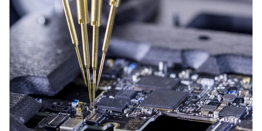
A passive probe with a long ground lead can create visible ringing even if the board is fine. A high-impedance or fast-edge node may need an active probe or differential approach. Before blaming the PCB, verify whether the measurement method itself is adding artifacts.
3. Keep the physical connection short and intentional
Probe attachment, test-point geometry, connector access, and reference ground location all matter. If the board is dense, HDI PCB or high-speed PCB layouts may need dedicated debug points designed in from the start instead of improvised during lab bring-up.
How triggering and setup discipline reduce false conclusions
Many failed debug sessions are not caused by bad hardware. They are caused by poor capture discipline. A scope that is free-running, over-triggering, or connected through a noisy probe path can make a healthy design look unstable.The most common setup problems are:
- edge triggers that are too loose to isolate a rare startup or fault event
- insufficient pre-trigger or record length for understanding what happened before the failure
- attenuation or scaling mismatches between probe and channel settings
- measurements taken from poor ground references or through unsafe floating connections
- comparing waveforms without keeping probe method and channel setup constant
If the board is part of a high-speed or mixed-signal program, oscilloscope work should be connected to the actual design review path, not treated as an afterthought. That usually means aligning high-speed PCB, SMT assembly, and PCB prototype planning before the first lab session starts.
What PCB teams should prepare before prototype bring-up
An oscilloscope becomes much more useful when the board was designed for measurement. Before prototype release, teams should define what must be measurable on day one and how that access will be created.A practical bring-up plan usually includes:
- Critical-node list
Identify rails, clocks, resets, enables, buses, and switching nodes that must be checked during first power-up. - Test-point strategy
Add accessible and labeled points where waveform integrity matters instead of relying on solder-mask scraping or unsafe probe attachment. - Measurement sequence
Decide the order of power-up checks, expected waveform behavior, and stop conditions if a rail or timing event looks wrong. - Probe and fixture plan
Confirm which channels, probes, adapters, and grounding methods are required before the board reaches the lab. - Revision and BOM control
Keep clear records of assembly version, component substitutions, and firmware state so measurements can be compared across builds. A BOM viewer review helps catch avoidable mismatches before bring-up.
If the project needs fast iteration between fabrication, assembly, and lab debugging, turnkey assembly and quick-turn PCB support usually reduce delays caused by fragmented handoffs.
FAQ
What is the first thing to check before measuring a PCB with a digital oscilloscope?
Check the actual measurement goal, expected signal range, required bandwidth, probe type, and where the ground reference will be taken. A good setup starts before the probe touches the board.
Does a higher-bandwidth oscilloscope always give a better PCB measurement?
Not automatically. More bandwidth can help with fast signals, but poor probing, bad grounding, or the wrong trigger setup can still make the measurement misleading.
Why do oscilloscope readings sometimes show ringing that may not be on the PCB?
Because long probe ground leads, poor tip connection, or measurement-loop inductance can create artifacts. Always verify the probing method before treating the waveform as a board defect.
When should a team use a differential probe instead of a standard passive probe?
Use a differential probe when measuring floating nodes, high-side signals, or situations where common-mode noise and safe referencing make a standard passive probe unreliable or unsafe.
What should be frozen before first prototype bring-up?
Freeze the critical-node list, test-point access, probe plan, trigger approach, expected startup sequence, and the record of which assembly revision is being measured.
Next steps
If you are preparing a PCB prototype for oscilloscope-based debug, the most useful next step is usually to review test access, bring-up order, and probing assumptions before the board is built.HILPCB can support that process through:
- HDI PCB review when dense routing threatens measurement access
- High-speed PCB planning when waveform integrity and edge behavior matter
- SMT assembly and turnkey assembly alignment when prototypes need consistent build quality for lab comparison
- PCB prototype and quick-turn PCB support for fast debug cycles
- Request a quote when your files, BOM, and bring-up notes are ready for review