
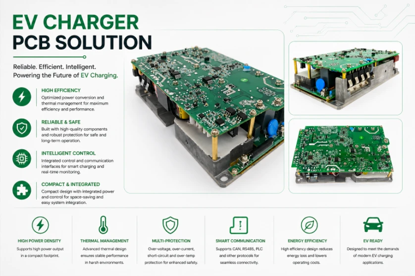
A 350 kW DC fast charger pushes 500 A at 800 V through silicon carbide switches operating at 50–100 kHz, generating voltage slew rates above 50 V/ns. The control board simultaneously manages CCS2 or NACS handshake protocols over PLC-based communication, monitors pilot signal duty cycles for current limit negotiation, measures insulation resistance in real time per IEC 61851, and streams usage data to a cloud OCPP 2.0.1 backend. Meanwhile, the charger sits outdoors year-round, cycling from -30°C winter nights to +50°C summer afternoons with direct sun exposure, surviving lightning-induced surges on both the AC mains and the DC output cable.
HILPCB manufactures EV charger PCBs from compact Level 2 wallbox controllers through multi-module DC fast charger power stages, using heavy copper fabrication up to 10 oz, high-voltage PCB isolation engineering, and multilayer constructions up to 64 layers for integrated power+control architectures.
Menu Navigation
- Power Stage Layout for SiC and GaN Topologies
- 800V Isolation Architecture on the PCB
- Communication and User Interface Boards
- Thermal Engineering for Outdoor Deployment
- EMC and Surge Protection
- Charger Manufacturing and Certification
Power Stage Layout for SiC and GaN Topologies
DC fast chargers use multi-stage conversion: active front end (PFC), isolated DC-DC stage (LLC resonant, DAB, or CLLC), and output regulation. Level 2 AC chargers are simpler — the vehicle's onboard charger handles AC-DC conversion, so the EVSE PCB manages only pilot signaling, relay control, and energy metering. But DC fast chargers contain the full power conversion chain, making their PCB layout a power electronics design challenge.
Power Board Design
- SiC Half-Bridge Switching Loop: SiC MOSFETs (Wolfspeed C3M, Infineon CoolSiC, Onsemi EliteSiC) switch at dV/dt rates of 30–80 V/ns. The half-bridge loop — from DC bus ceramic capacitors through high-side FET, switching node, low-side FET, back to capacitors — must achieve <2 nH total loop inductance. Components placed directly adjacent on the same layer. Bus ceramics (22 µF × 4–8, C0G or X7R with DC bias derating to actual capacitance at operating voltage) placed within 3 mm of the FET drain-source connections. Heavy copper layers (3–6 oz external, 2–3 oz internal) for power paths.
- Gate Driver Kelvin Source: SiC gate drivers require a dedicated Kelvin source (sense) connection — a separate low-current return path from the MOSFET source pad, independent from the power source carrying load current. This prevents di/dt-induced voltage on the power source from fighting the gate drive voltage. On the PCB, the Kelvin source trace routes on a separate layer from the power source plane, connecting only at the MOSFET's source sense pin.
- LLC Resonant Tank: The resonant inductor and capacitor in an LLC converter see AC currents at the resonant frequency (80–150 kHz typically). The PCB traces connecting these components carry high AC current — 20–50 Arms at 100 kHz — requiring wide copper pours with sufficient cross-section to maintain Q-factor. High trace resistance degrades LLC efficiency and shifts the resonant frequency.
- Transformer Interface: Primary-secondary isolation in the DC-DC stage provides the required galvanic isolation. Primary winding connections and secondary winding connections to the PCB must maintain ≥8 mm creepage for reinforced insulation at 800 V working voltage. Physical slot isolation between primary and secondary sections of the board.
800V Isolation Architecture on the PCB
DC fast chargers handle 800+ V DC output and 480 V AC input simultaneously. IEC 61851-23, UL 2202 (Level 2), UL 2594 (DC), and regional standards define the isolation requirements.
Isolation Implementation
- Creepage Engineering: Reinforced insulation between mains-referenced and vehicle-referenced circuits — ≥10 mm creepage at 1,000 V working voltage on Material Group IIIb laminate (standard FR-4). CNC-routed slots (2.0–3.0 mm width) where board area doesn't permit surface gaps. HILPCB holds slot width to ±0.1 mm with solder mask pullback preventing glass fiber tracking along cut edges.
- High-CTI Materials: Laminates with CTI ≥ 600 (Material Group I) allow significantly reduced creepage distances at the same working voltage — enabling compact module designs that would be physically impossible on standard FR-4. HILPCB stocks high-CTI automotive-grade laminates from Isola and Panasonic with lot-level incoming inspection.
- Internal Isolation Barrier: A dedicated prepreg layer (≥0.5 mm cured thickness) between primary and secondary copper prevents dielectric breakdown through the board. No via barrel penetrates this barrier. Hi-pot tested at 4,500 V AC per production panel — 100% testing, no sampling.
- Isolation Monitoring Circuit: DC fast chargers continuously measure insulation resistance between DC output and ground per IEC 61851-23. The monitoring circuit's own PCB routing must not compromise the safety isolation boundary — measurement injection and sensing traces routed within the safety-rated isolation zone with appropriate creepage from both primary and secondary circuits.
Communication and User Interface Boards
The charger's intelligence resides on a separate control/communication board — managing vehicle handshake, user authentication, energy metering, and backend connectivity.
Control Board Functions
- Pilot Signal and Proximity: SAE J1772 / IEC 61851-1 pilot signal (±12 V, 1 kHz PWM) communicates available current. Proximity detection (PP pin) confirms connector insertion and cable rating. These signals operate at low voltage but their timing accuracy directly affects the vehicle's current draw — a PWM duty cycle error of 2% can cause the vehicle to draw 1–2 A more than the EVSE's circuit breaker rating.
- CCS/NACS Digital Communication: CCS PLC-based communication (ISO 15118) runs over the CP line or dedicated PLC pins. The modem IC's coupling circuit connects to the charging cable through a transformer — PCB traces between modem and coupling transformer maintain impedance matching for the PLC signal band (2–30 MHz for HomePlug Green PHY). For NACS connectors with ISO 15118 over PLC, the same coupling circuit applies.
- OCPP Backend Connectivity: 4G/LTE cellular modem or Ethernet for OCPP 1.6J/2.0.1 connection to the Charge Point Management System. Cellular modules require controlled-impedance antenna feed (50 Ω) and power supply capable of supplying 2 A peak during TX bursts without sagging the rest of the control board's supply.
- Revenue-Grade Energy Metering: MID-certified (EU) or ANSI C12 (US) energy measurement for billing accuracy. Metrology front end — shunt or CT current sensing with Kelvin connections, voltage divider with ±0.05% accuracy, and dedicated metering IC with anti-tamper features. PCB layout following the same isolation and grounding principles as utility smart meters.
- User Interface: TFT display, NFC/RFID reader (ISO 14443A/B for credit card payment, ISO 15693 for fleet cards), LED status indicators, and emergency stop button interface. These circuits operate at safe extra-low voltage (SELV) and must maintain isolation from both AC mains and DC output sections.
Thermal Engineering for Outdoor Deployment
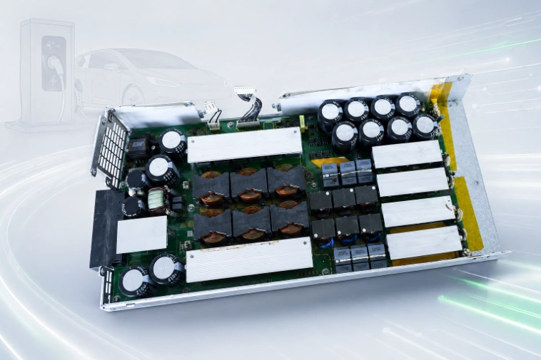
Chargers operate outdoors from -30°C to +50°C ambient (wider than automotive -40°C to +85°C in many specs). Internal power dissipation raises board temperatures further. Many commercial units use sealed IP54/IP55 enclosures without rotating fans — relying on natural convection and conduction cooling.
Thermal Solutions on the PCB
- Copper Heat Spreading: Heavy copper planes (3–4 oz) distribute heat from power devices across the board area. Thermal via arrays (0.3 mm drill, 0.6 mm pitch, copper-filled) under MOSFETs and rectifier diodes transfer heat to the opposite board surface where it conducts through thermal pads to an aluminum heatsink or the enclosure wall.
- High-Tg Materials: Tg ≥ 170°C with Td ≥ 340°C for lead-free assembly profiles and sustained high-temperature operation. At full power in a sealed enclosure on a hot day, board temperatures can reach 120–130°C at power device locations. Standard 140°C Tg FR-4 is at or beyond its glass transition under these conditions — causing dimensional instability and accelerated aging.
- Conformal Coating: Automotive-grade acrylic or silicone coating (25–75 µm) protecting assembled boards from condensation during nighttime temperature drops, road splash, de-icing chemicals, and bird droppings (which are surprisingly corrosive). Coating must not cover high-current relay contacts, power terminal connections, or thermal pad interfaces.
- Thermal Simulation Coordination: HILPCB provides copper weight, layer stack-up, via array density, and board geometry data in formats compatible with thermal simulation tools (Ansys Icepak, Siemens FloTHERM). This ensures the manufactured board's actual thermal performance matches the modeled prediction — preventing thermal surprises during charger certification testing.
EMC and Surge Protection
SiC converters switching at 50–100 kHz with 30+ V/ns edges generate broadband conducted and radiated emissions from fundamental through 200+ MHz. Additionally, chargers connected to the AC grid and the DC charging cable are exposed to lightning-induced transients on both interfaces.
EMC and Surge Design
- Input EMI Filter Layout: Common-mode and differential-mode filter stages at the AC board entry point. Filter components placed close together and close to the input connector — long PCB traces between filter stages become unintentional antennas that bypass the filter. Ground connections for Y-capacitors routed directly to the safety earth trace, not through the circuit ground plane.
- Output EMI Filter: The DC output cable radiates switching harmonics into the environment. Output LC filtering and common-mode choke placement on the DC output board suppress conducted emissions below CISPR 32 Class B limits. Cable ferrites complement board-level filtering for frequencies above 30 MHz.
- Surge Protection: IEC 61000-4-5 requires 4 kV (1.2/50 µs) surge withstand on AC mains ports and 2 kV on DC output ports. MOVs and TVS diodes at board entry points — traces rated for surge current (>100 A peak for <50 µs) without fusing. Via connections from surge protection components to the ground plane sized for peak surge current.
- Switching Loop EMI: Every dB of EMI reduced by layout compactness (shorter traces, smaller loop areas) saves a component in the EMI filter — directly reducing BOM cost, board space, and weight. The most effective EMI suppression strategy is making the switching loop inductance as low as possible, not adding more filter components.
Charger Manufacturing and Certification
Production for Charger OEMs
- Prototype: 5–25 boards for type testing per IEC 61851, UL 2202/2594, and regional certification requirements. DFM review identifying isolation, thermal, and manufacturing risks before first article.
- Pilot Production: 200–2,000 units with PPAP documentation for automotive-grade charger OEMs. Process validation (IQ/OQ/PQ) for critical solder joints and isolation barriers.
- Volume Production: 5,000+/year with automated ICT, hi-pot testing (100% at rated test voltage), functional verification, and SPC monitoring on critical characteristics. Full lot traceability supporting charger warranty and field service programs.
Submit your EV charger design for isolation review and manufacturing quote →
Frequently Asked Questions
How does EV charger PCB layout handle 800V architectures? 800V DC fast chargers require reinforced insulation and significant creepage distances (often ≥10 mm on standard FR-4). HILPCB uses CNC-routed isolation slots and high-CTI (Comparative Tracking Index ≥ 600) laminates to meet safety requirements while keeping power module designs compact.
What are the thermal challenges for EV charger PCBs? EV chargers operate outdoors in extreme environments (-30°C to +50°C) while dissipating significant internal heat from SiC or GaN power switching. The PCB addresses this through heavy copper planes (up to 10 oz) for heat spreading, thermal via arrays under power devices, and high-Tg materials that remain stable at elevated operating temperatures.
Why is a Kelvin source connection important for SiC gate drivers? SiC MOSFETs switch at extremely high dV/dt rates. A Kelvin source connection provides a dedicated, low-current return path for the gate driver, completely separate from the power source path carrying the load current. This prevents voltage drops caused by high di/dt from interfering with the gate drive signal.
What conformal coating is recommended for outdoor EVSE PCBs? Automotive-grade acrylic or silicone conformal coatings (25–75 µm thick) are heavily recommended for outdoor charger boards. These coatings protect the PCB from condensation, high humidity, salt spray, and corrosive environmental contaminants that can cause leakage currents or short circuits.