
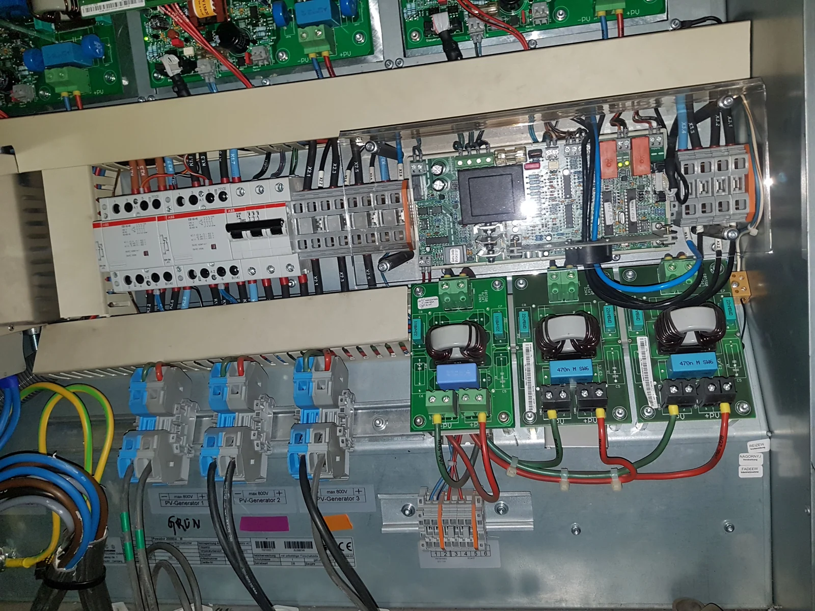
- What should be frozen first in OBC PCB design is not detailed component placement, but whether the high-voltage area, low-voltage control area, power loops, and thermal paths already form clear boundaries. If those boundaries are still changing late in layout, EMC, assembly, and validation will all start to drift together.
- An OBC is not just an enlarged DC-DC board. IEC 60664-1 clearly provides the principles and test context for insulation coordination, clearance, creepage distance, and solid insulation in low-voltage supply systems. That means an OBC board has to be handled as an insulation-coordination problem first, before routing optimization.
- Power loops and sensing returns cannot be reviewed separately. UNECE R10 is the public regulatory entry point for vehicle EMC, and on an OBC board many conducted and radiated problems are not simply caused by an "insufficient filter," but by high di/dt loops, interface entries, and sensitive return paths not being separated on the PCB.
- Thermal issues cannot be left to the heatsink alone. The copper distribution, vias, and assembly flatness between power devices, the DC link, inductors, shunt resistors, and thermal interfaces are already part of the OBC thermal path.
- What really deserves approval is not "this board works," but "this insulation, loop, thermal, and assembly logic can be manufactured repeatedly and validated consistently."
Quick Answer
The core of EV on-board charger OBC PCB design is to put insulation coordination, power switching loops, thermal spreading, sensing returns, and automotive development discipline into one board-level input set. For a high-voltage EV charger board, freezing boundaries and the validation matrix early is more effective than trying to recover later through EMC or thermal rework.
Table of Contents
- What should engineers review first on an OBC PCB?
- Summary table of key rules and parameters
- Why must insulation zoning and creepage distance be defined before layout refinement?
- Why do power loops and sensing returns go out of control first?
- Why must thermal paths and assembly flatness be reviewed together?
- Why must OBC projects be introduced through a validation matrix and development discipline?
- Next steps with HILPCB
- Frequently Asked Questions (FAQ)
- Public references
- Author and review information
What should engineers review first on an OBC PCB?
Start with insulation boundaries, the main power loop, thermal paths, sensing returns, EMC entry points, and the validation matrix.
This does not mean "route the schematic first and add safety spacing later," and it does not mean "get the sample board running first and deal with automotive convergence afterward." The public description of IEC 60664-1:2020 makes clear that it provides insulation-coordination principles, requirements and tests for equipment within low-voltage supply systems, including the evaluation of clearances, creepage distances, and solid insulation. UNECE Regulation No. 10 is the public regulatory entry point for vehicle EMC. Put together, these public materials lead to a straightforward engineering conclusion: an OBC board has to stand up geometrically and by zoning first. Only then do efficiency, EMC, and thermal behavior have a real basis for convergence.
Before stackup and layout freeze, the five questions that are usually most useful are:
- Are the high-voltage power area, low-voltage control area, and interface area already physically separated?
- Do the main switching loop, DC link, and rectification/output loop form the shortest possible closed paths?
- Can heat from hotspot devices spread into effective copper layers, vias, and structural parts?
- Do sensing, drive, and communication returns avoid high-noise areas?
- Have material, assembly, traceability, and validation inputs already been prepared as executable engineering files?
If the project starts with high voltage, high heat-flux density, and a large mixed assembly of components, it is usually better to bring the structural limits of Multilayer PCB and Heavy Copper PCB into the OBC review early, instead of trying to reverse-engineer the manufacturing window after the power area is already laid out.
Summary table of key rules and parameters
| Rule / Parameter | Recommended range or judgment method | Why it matters | How to verify | What happens if ignored |
|---|---|---|---|---|
| Insulation boundary | Define zoning first according to working voltage, pollution conditions, and structural tolerances | OBC is constrained first by insulation coordination | Creepage/clearance review, structural cross-review | The sample works, but hipot or vehicle testing fails |
| Power loop | Keep input capacitor, switching devices, magnetic parts, and return planes tightly coupled | Determines spikes, EMI, and local temperature rise | Layout review, oscilloscope, near-field testing | Debug becomes difficult and EMI rework repeats |
| Sensing return | Plan sensing points and control ground according to real physical loops | Prevents high noise from contaminating the control chain | Waveforms, false-trigger analysis, return-path review | Protection misfire, drift, and instability |
| Thermal path | Heat must move from the device into copper, vias, and mechanical interfaces | A heatsink cannot compensate for board-level thermal bottlenecks | Thermal imaging, temperature-rise testing, cross-section analysis | Hotspots, solder stress, and reduced lifetime |
| Assembly window | Review thick copper, large pads, terminals, and coating areas together | Directly affects soldering and rework | First-article inspection, X-ray, flatness check | Bare board passes, but assembly is unstable |
| Development discipline | Move validation, traceability, and document control forward | Automotive introduction is not just "add a few more tests" | Document review, version tracking, pilot review | Prototype logic and production logic disconnect |
| Typical situation | What should be prioritized |
|---|---|
| High-voltage isolated OBC main power board | Insulation zoning, power loop, hotspot spreading |
| OBC with control and power on the same board | Sensing returns, noise zoning, interface boundaries |
| High-power-density compact board | Board thickness, copper weight, flatness, thermal interface coordination |
Why must insulation zoning and creepage distance be defined before layout refinement?
Conclusion: Because the first constraint on an OBC board is high-voltage insulation, not routing elegance or component density.
The public description of IEC 60664-1 already makes clear that it addresses insulation coordination for equipment within low-voltage supply systems and provides the framework for evaluating clearances, creepage distances, and solid insulation. For a high-voltage automotive board like OBC, this means the high-voltage power area, low-voltage control area, connector boundaries, slots, insulation coating, and pollution environment cannot be postponed until later.
What is worth freezing first includes:
- The physical boundary between the high-voltage power area and the low-voltage control area
- The real manufacturing margin around connectors, transformers, sensing devices, and isolation devices
- Whether slots, insulation barriers, and structural parts conflict with each other
- Which areas need to be handled under stricter environmental or assembly conditions
If the project also includes nearby structural parts, condensation risk, or complex connector exits, manufacturing tolerances and processing boundaries from PCB Manufacturing should usually be brought into the insulation review at the same time instead of judging only by nominal CAD dimensions.
Why do power loops and sensing returns go out of control first?
Conclusion: Because the power stage and control stage on an OBC board are naturally coupled, and once noisy loops are not kept clean in layout, they contaminate sensing and drive circuits first.
UNECE R10 is a vehicle-level EMC regulation, but its direct meaning for an OBC PCB is clear: switching-node area, interface entry, filter position, and return path have to be managed early, or many of the issues later seen in the lab are simply the result of board geometry amplifying them. In a high di/dt power loop, if the input capacitor, main switching devices, rectification path, and return plane are not kept tightly coupled, noise will follow the shortest parasitic route back into the sensing and control network.
What deserves the earliest confirmation is:
- Whether the main power loop has already been compressed enough
- Whether high-frequency decoupling is placed where it is electrically effective
- Whether sensing ground, drive ground, and high-current returns are actively planned
- Whether interfaces, communication lines, and sensitive control traces avoid fast-switching nodes
If the project is validating a high-power sample board, it is usually better to include the assembly reality of SMT Assembly in the review as well, because component height, terminal position, and real solder state also change return paths and parasitics.
Why must thermal paths and assembly flatness be reviewed together?
Conclusion: Because thermal issues inside an OBC board usually appear first as solder stress, local hotspots, and assembly instability, not simply as "component temperature is high."
Many OBC projects think of thermal design as heatsink selection, but the real result is decided earlier by the PCB. The bottom pads of power devices, copper spreading, thermal vias, local copper weight, contact surfaces to structural parts, and coplanarity of large components all determine how heat leaves the board. If any part of that path is discontinuous, external thermal hardware cannot fully compensate.
A more realistic thermal review usually includes:
- Whether hotspot devices have truly effective copper spreading regions nearby
- Whether thermal vias connect to effective layers instead of isolated copper islands
- Whether thick copper and large copper areas amplify warpage or uneven reflow
- Whether heatsinks, insulation pads, or enclosure contacts demand tighter flatness
If heat-flux density is high, it is usually better to compare the manufacturing and assembly windows of Heavy Copper PCB and High Thermal PCB together rather than deciding only from thermal conductivity in isolation.
Why must OBC projects be introduced through a validation matrix and development discipline?
Conclusion: Because automotive readiness is not just adding a few more tests. It means turning design assumptions, manufacturing inputs, assembly constraints, and validation results into one traceable closed loop.
ISO's public introduction describes ISO 26262 as a complete standards package for road vehicles functional safety, covering concept, system, hardware, software, production, supporting processes, and guidelines. For an OBC project, that does not mean PCB design must copy every clause literally. It means key boundaries, key structures, key validations, and change logic cannot rely on verbal alignment.
A more valuable pre-release validation matrix usually includes:
- Insulation-boundary verification. Creepage, clearance, slots, and structural boundaries are bound to drawing revision.
- Power-loop verification. Key loop waveforms, noise behavior, and interface-zone condition are included in sample-board checks.
- Thermal-path verification. Thermal images, hotspots, solder joints, and assembly flatness are reviewed together.
- Assembly verification. Thick-copper zones, terminal areas, large pads, and key-device checkpoints are clearly defined.
- Document and traceability verification. Stackup, Gerber, BOM, coating notes, and manufacturing instructions stay under one controlled version.
If the project is already approaching first build or pilot production, it is usually better to organize these inputs directly into Quote / RFQ and pilot engineering notes rather than leaving the question of "what must be validated" until after the line starts.
Next steps with HILPCB
If you are working on an EV on-board charger, a DCDC/OBC power board, or another high-voltage automotive power-electronics project, the next step is usually to turn "Is the design usable?" into "Are the boundaries manufacturable, assemblable, and verifiable?"
- When the main problem is high-voltage zoning and layer structure, first use the Multilayer PCB path to converge stackup and zoning.
- When hotspots, current, and copper weight have become the main constraints, first verify the process windows of Heavy Copper PCB and High Thermal PCB.
- When the project is preparing for high-voltage sample validation, moving key structures into PCB Prototype makes it easier to reveal issues early.
- When fabrication and assembly limits will directly affect the performance of power devices and terminals, bring SMT Assembly into the review at the same time.
- Once stackup, power loops, insulation boundaries, and the validation matrix are frozen, organizing them into Quote / RFQ improves engineering communication.
Frequently Asked Questions (FAQ)
What risk on an OBC PCB is most often underestimated?
A: Usually not a single device parameter, but the coupling between the high-voltage insulation boundary, the main power loop, sensing returns, and thermal paths.
Can high-CTI or higher-grade materials replace proper insulation zoning?
A: No. Material properties matter, but they cannot replace physical separation, manufacturing tolerance control, slots, and structural-boundary control.
Why do many OBC thermal problems appear only after pilot build?
A: Because real assembly, real thermal interfaces, and production-level reflow magnify local hotspots, warpage, and solder stress. Those effects are not always fully visible at the early sample stage.
Does automotive readiness just mean running more tests?
A: No. More fundamentally, it means turning design, documentation, validation, and traceability into a single closed loop. Testing is only one proof point inside that loop.
What is most worth freezing before fabrication?
A: Prioritize insulation boundaries, power loops, thermal paths, sensing returns, assembly limits, and the validation matrix. The later these inputs are frozen, the higher the rework cost.
Public references
IEC 60664-1:2020 | Insulation coordination for equipment within low-voltage supply systems
Supports the article's explanation that IEC 60664-1 publicly provides insulation coordination principles plus the context for clearances, creepage distances, solid insulation, and testing.UN Regulation No. 10 - Rev.6 - Amend.1 | UNECE
Supports the article's point that UNECE R10 is the public regulatory entry point for vehicle EMC and that OBC projects must bring EMC entry control and board zoning forward.ISO 26262 road vehicles functional safety
Supports the article's explanation that ISO 26262 covers a full functional-safety development context including concept, hardware, software, production, and supporting processes.48V in automotive design resources | TI
Supports the public context that 48V automotive power solutions must minimize both heat dissipation and EMI, which also serves as background for OBC and automotive power-electronics board constraints.
Author and review information
- Author: HILPCB Power Electronics and Automotive Board Content Team
- Technical review: PCB process, insulation design, thermal design, and assembly engineering team
- Last updated: 2026-05-17