
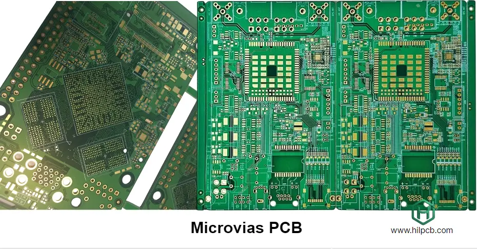
With the explosive growth of AI and high-performance computing (HPC), the bottleneck of data processing has moved from compute units to the “last mile” of data transfer: die-to-die interconnect. HBM3—and what follows it—delivers extraordinary memory bandwidth and is central to breaking that bottleneck. But integrating a powerful AI processor with HBM3 stacks seamlessly requires a seemingly small yet mission-critical component: the interposer. Achieving excellent HBM3 interposer PCB quality is no longer optional; it is the foundation for stable, efficient operation of the entire AI system. As an engineer focused on thermal interfaces and tolerance control, I know that in a micron-scale world, even tiny deviations can cause cliff-edge performance loss—or outright system failure.
This article breaks down the core elements behind HBM3 interposer PCB quality—from high-speed SI and harsh thermal management to PDN complexity and manufacturing execution. Understanding how HILPCB helps optimize your AI interconnect/substrate design can be a decisive step toward success.
Why HBM3 interconnect places unprecedented requirements on interposer PCBs
Each generation of HBM increases data rate and channel density dramatically. From HBM2e to HBM3, data rate doubles, pins per stack exceed 1024, and total bandwidth reaches TB/s class. That performance leap translates directly into extreme requirements on the HBM3 interposer PCB that carries and connects those signals.
First, physical scaling is brutal. The interposer must place tens of thousands of micro-bumps in a very small area (often only a few hundred mm²), connecting the SoC and HBM stacks above while fanning down into the package substrate. Pitch is already in the micron range—pushing routing density and manufacturing accuracy toward wafer-like expectations.
Second, electrical requirements rise sharply. Beyond 6.4 Gbps, every micron-scale trace on the interposer behaves like a precision transmission line. Small geometry error or dielectric inconsistency creates attenuation, reflection, and crosstalk—directly impacting data correctness. Building a qualified low-loss HBM3 interposer PCB therefore becomes a first-order design goal.
Finally, the interposer is no longer “just” an electrical platform. At the center of 2.5D packaging, it becomes a core hub for thermal and power transfer. Massive heat from the AI die and HBM stacks must flow through it, while stable, clean current must be delivered through it to the silicon. Interposer design becomes a multi-physics co-design problem across electrical, thermal, and mechanical domains.
How do you maintain signal integrity (SI) on micron-scale routing?
At HBM3 data rates, SI is the primary electrical metric behind HBM3 interposer PCB quality. Interposer routing lengths are short (often millimeters), but extreme density and speed make SI unusually complex.
1. Precise impedance control: HBM3 channel impedance must stay within a tight target (e.g., 50 Ω). With line widths under 10 µm, tiny etch error, dielectric thickness variation, or copper thickness drift can push impedance off target. This requires advanced manufacturing (mSAP or SAP) to control geometry tightly. It also requires materials with extremely stable Dk and Df across frequency.
2. Strict crosstalk management: Thousands of lines run in parallel at tiny spacing. You must suppress NEXT and FEXT via routing optimization, ground shielding, and precise spacing control. SI tools are essential early to predict and avoid crosstalk pitfalls.
3. Minimize insertion loss and return loss: Dielectric and conductor loss attenuate signals (Insertion Loss). Ultra-low Df dielectrics such as Ajinomoto Build-up Film (ABF) are key to building low-loss HBM3 interposer PCB. Discontinuities (vias, pads) create reflections (Return Loss). Via structures, pad geometry, and micro-bump transitions must be optimized to preserve eye quality—where deep experience with high-speed PCB principles matters.
Interposer substrate material comparison
| Metric | Standard FR-4 | High-speed laminates (e.g., Megtron 6) | ABF build-up film |
|---|---|---|---|
| Dk @10GHz | ~4.5 | ~3.6 | ~2.8 - 3.2 |
| Df @10GHz | ~0.020 | ~0.002 | ~0.001 - 0.002 |
| Min line/space | > 75µm / 75µm | ~ 25µm / 25µm | < 10µm / 10µm |
| Thermal conductivity (W/m·K) | ~0.3 | ~0.6 | ~0.4 |
| Typical use | Conventional PCBs | High-end server motherboards | HBM interposers, IC substrates |
What thermal management strategies work under massive AI chip power?
As a thermal-interface engineer, I must emphasize: thermal management is central to HBM3 interposer PCB reliability and long-term performance. An AI accelerator consuming hundreds of watts (even approaching kilowatts at system level) can reach extreme heat flux. The interposer sits at the center of this “thermal storm.”
1. Efficient vertical conduction paths: The interposer must function as a high-efficiency thermal conduit. Designs use dense Thermal Vias—filled micro-channels that act like tiny heat pipes—to conduct heat into the package substrate and heatsink. Via density, diameter, and fill material directly affect thermal performance.
2. Thermal properties of materials: Organic interposers (ABF-based) can be attractive for electrical performance and cost, but thermal conductivity is far lower than silicon interposers. To compensate, organic designs often embed large continuous copper planes as thermal spreading layers. Copper thickness and continuity are critical for lateral heat spreading.
3. TIM and coplanarity/warpage control: Thermal transfer depends heavily on interface quality. From HBM to interposer to substrate, each interface uses TIM. TIM performance requires flatness and contact pressure. Warpage is the enemy: even a few microns of bow can create uneven TIM thickness, hotspots, and ultimately HBM throttling or damage. This is why HBM3 interposer PCB quality—especially warpage control—directly determines thermal success. Manufacturers like HILPCB control warpage through symmetric stackup, strict lamination control, and materials selection to meet tight tolerances.
How does power integrity (PI) impact HBM3 stability?
If SI ensures data “clarity,” PI ensures the system “heartbeat.” During large-scale parallel compute, AI chips draw rapidly changing current that creates transient noise.
1. Ultra-low-impedance PDN: The HBM3 interposer PCB must provide extremely stable, low-impedance power delivery to the SoC and HBM—typically by dedicating multiple power and ground planes in the stackup. These planes behave like a large capacitor, responding quickly to transient current demand and suppressing voltage droop.
2. Carefully designed decoupling network: High-frequency noise requires extensive decoupling. On space-constrained interposers, Embedded Capacitance may be used to integrate capacitance layers directly into the stackup to minimize current-loop length and improve decoupling efficiency.
3. Minimize loop inductance: Current flows from power planes to the die and returns through ground planes, forming loops. Lower loop inductance means faster transient response and less voltage noise. Plan power/ground via placement tightly to minimize loop area. Strong HBM3 interposer PCB PDN can achieve milliohm-level impedance in the target band.
💎 Interposer PDN: golden rules for advanced-package power distribution
Optimize vertical interconnect between silicon interposer and substrate to eliminate core voltage fluctuation
Core strategy: Deploy Deep Trench Capacitors (DTC) or micro-capacitor arrays as close as physically possible to chiplets. Increase local charge storage to provide sub-nanosecond current compensation for GHz switching activity.
Core strategy: Use TSV arrays to build short power paths. Optimize RDL width-to-length ratios and compress loop area to micron scale using tightly stitched, interleaved power/ground vias.
Core strategy: Build continuous power and ground reference planes across layers. Use very thin dielectric thickness to create large inter-plane capacitance, providing an ultra-low-impedance return path for high-frequency noise.
Core strategy: Run end-to-end CPM (Chip Power Model) co-simulation from die to package base. Predict SSN and DC IR-Drop accurately, then optimize routing density under thermal-stress constraints.
For high-compute chips, we provide high-precision RDL (Fine Pitch Line/Space) and Micro-bump manufacturing support. By tightly controlling dielectric thickness and copper pillar alignment, HILPCB helps you build interposer solutions with excellent PI that meet the harsh dynamic power demands of AI and HPC.
Which manufacturing processes determine HBM3 interposer PCB reliability?
Even a perfect design needs top-tier process execution. HBM3 interposer PCB reliability depends on manufacturing precision and consistency—beyond traditional PCB and closer to semiconductor packaging—so it is typically built by specialized IC Substrate PCB manufacturers.
1. Fine-line fabrication: Below 10 µm line/space, subtractive processes are insufficient. SAP/mSAP must be used. These build traces via lithography and plating on thin copper, achieving near-vertical sidewalls and very high dimensional accuracy.
2. Microvia drilling and via fill: Layer transitions rely on laser-drilled microvias (typically 20–30 µm). Drill quality, hole-wall cleanliness, and uniform via fill are critical for long-term interconnect reliability. A single microvia failure can break an HBM channel.
3. Lamination and registration accuracy: Multilayer interposers require extremely tight registration—often within a few microns. Misregistration can cause via-to-pad opens/shorts. This demands top registration systems plus strict environmental controls (temperature, humidity, cleanliness).
4. Warpage control: Warpage is a central interposer challenge. Manufacturers like HILPCB reduce warpage via optimized symmetric structures, low-CTE core materials, and precision lamination parameters to ensure high yield in downstream packaging flows such as CoWoS.
How do you balance performance, cost, and quick-turn lead time?
In the competitive AI market, time-to-market drives demand for HBM3 interposer PCB quick turn. Yet interposer complexity seems at odds with “quick.”
Balancing performance, cost, and cycle time is a systems problem:
- Performance first: For top-tier accelerators, performance is non-negotiable—requiring the most advanced materials/processes, with higher cost and longer lead time.
- Cost optimization: For cost-sensitive applications, discuss slightly lower-performance but more cost-effective materials, or simplify design to reduce layer count and process complexity.
- Fast delivery: HBM3 interposer PCB quick turn depends on engineering capability and process management. Strong DFM engagement early avoids manufacturing traps and reduces design spins. Mature processes, stable supply chains, and efficient scheduling shorten lead time.
As a manufacturer offering one-stop service from prototype to mass production, Highleap PCB Factory (HILPCB) operates with this balance in mind. Through tight early technical collaboration and flexible line configurations, we provide competitive prototype assembly and quick-turn builds while maintaining top-tier quality.
HILPCB IC substrate and interposer manufacturing capability overview
| Parameter | Capability | Parameter | Capability |
|---|---|---|---|
| Max layers | 32+ Layers | Thickness range | 0.1 - 2.0 mm |
| Min line/space | 8µm / 8µm (SAP) | Min laser via | 25µm |
| Impedance tolerance | ±5% | Layer-to-layer registration | ±15µm |
| Supported materials | ABF, BT, high-speed laminates | Surface finish | ENEPIG, OSP |
Your HBM3 interposer PCB quality checklist
To ensure success systematically, we recommend using a structured HBM3 interposer PCB checklist across project phases. It is both a design guide and a communication tool with your manufacturer.
Design-stage checklist:
- Material selection: Low-loss materials (e.g., ABF) selected for SI and thermal needs?
- Stackup design: Symmetric stackup to control warpage? Sufficient and well-planned power/ground planes?
- SI simulation: Impedance/crosstalk/loss simulation validated for all HBM3 channels?
- PI simulation: PDN simulated; impedance meets target across frequency band?
- Thermal simulation: Hot spots identified and thermal-via design verified?
DFM-stage checklist:
- Line/space: Minimum geometry within manufacturer capability with margin?
- Via design: Microvia aspect ratio reasonable? Via-in-Pad compliant with process rules?
- Tolerance analysis: Manufacturing tolerance impact on impedance and timing considered?
- Warpage analysis: Warpage simulated jointly with manufacturer; stackup/panelization optimized?
Manufacturing and QA checklist:
- Trace inspection: 100% AOI on every layer?
- Registration verification: X-Ray verification on key layers?
- Impedance testing: TDR testing on test coupons (sampling or 100%) with report?
- Reliability testing: JEDEC-level thermal cycle, HAST, and other required reliability tests completed?
FAQ
Why is HBM3 interposer quality so critical for AI chip performance?
Because the interposer sits directly between the AI die, HBM stacks, and package substrate. Any weakness in signal routing, power delivery, thermal transfer, or dimensional control can reduce bandwidth, increase errors, or shorten long-term reliability.
What makes signal integrity so difficult on an HBM3 interposer?
HBM3 channels run at very high speed with extremely fine geometries and dense parallel routing. That combination makes impedance drift, crosstalk, return loss, and dielectric inconsistency much more damaging than on conventional PCBs.
Why does warpage control matter so much in HBM3 interposer manufacturing?
Even small warpage can disturb TIM contact, coplanarity, and downstream package assembly yield. It directly affects thermal performance, mechanical stress, and the consistency of micro-scale interconnect structures.
Which manufacturing processes most strongly influence HBM3 interposer reliability?
The biggest factors are fine-line SAP or mSAP fabrication, laser microvia quality, via fill consistency, tight lamination registration, and overall warpage control. These processes determine whether the design can be reproduced with stable electrical and mechanical quality.
Conclusion
The future of AI silicon starts with uncompromising execution on foundational components. HBM3 interposer PCB quality is far more than a manufacturing KPI—it is a synthesis of materials science, high-speed electronics, thermodynamics, and precision manufacturing. From micron-scale channels to system-level stability, every interposer detail influences AI performance and reliability.
To deliver a high-performance AI interconnect solution, designers must partner with manufacturers that have deep technical accumulation and advanced process capability. With years of experience in IC substrates and HDI, HILPCB provides one-stop services from design optimization and material selection to precision fabrication and assembly—helping customers meet the harshest requirements and ensuring your HBM3 interposer PCB reaches the highest quality standard.
Contact HILPCB to start your high-performance AI interconnect project and get a free DFM evaluation. Let’s build a solid hardware foundation for the future of AI.