
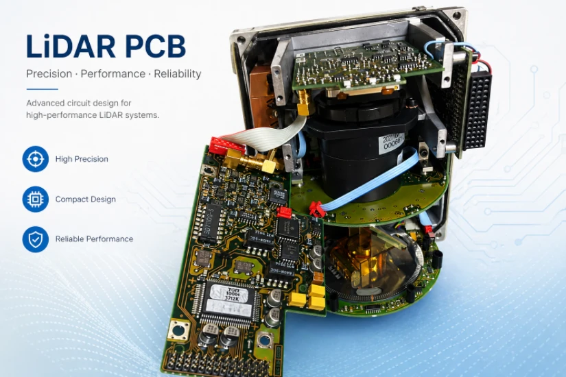
A LiDAR system fires 905 nm or 1550 nm laser pulses at 500 kHz–2 MHz repetition rates, detects photons arriving back 6.67 ns per meter of round-trip distance, and measures the return time with sub-nanosecond precision to build a three-dimensional point cloud of the environment. The PCB carries the laser driver delivering 5–50 A current pulses in 2–5 ns rise time, the transimpedance amplifier processing picoamp signals from avalanche photodiodes biased at 200+ V, the time-to-digital converter resolving 20–50 ps timing bins, and the FPGA computing the 3D point cloud at millions of points per second.
No other application demands simultaneous expertise in high-current nanosecond pulsing, sub-picoamp analog detection, picosecond-resolution timing, and real-time digital processing — on a single board surviving automotive vibration profiles and operating from -40°C to +105°C. The laser driver's 2 ns edges contain spectral energy through 200 MHz that, if not contained by the PCB layout, couples directly into the receiver's picoamp-sensitivity analog front end 15 mm away, swamping the reflected photon signal.
HILPCB manufactures LiDAR PCBs for autonomous vehicle developers, robotics companies, and surveying equipment OEMs using high-speed, heavy copper, and HDI fabrication. Our IATF 16949 manufacturing processes support automotive qualification requirements including PPAP documentation and accelerated reliability testing.
Menu Navigation
- Laser Driver Board: Nanosecond High-Current Pulses
- Receiver Front End: Detecting Single Photons
- Time-of-Flight Signal Chain and Processing
- TX-RX Isolation on a Shared Board
- Automotive and Industrial Qualification
- Architecture-Specific PCB Considerations
Laser Driver Board: Nanosecond High-Current Pulses
The laser driver must deliver 5–50 A peak current in pulses as short as 2 ns — then cut off completely before the receiver blanking window ends and detection begins. This demands GaN FET or high-speed Si MOSFET drivers with gate loop inductance below 0.5 nH and power loop inductance below 1 nH.
Laser Driver Layout
- Power Loop Compactness: The critical current loop — energy storage capacitor → switch (GaN FET) → laser diode → return to capacitor — must be physically as small as possible. Every nH of loop inductance at 50 A creates a 50 V spike at turn-off (V = L × di/dt, with di/dt ≈ 50 A/2 ns = 25 GA/s). These spikes destroy the laser diode if they exceed its absolute maximum reverse voltage. Ceramic bus capacitors (10–100 nF, rated 100–200 V, C0G dielectric for sub-nH ESL) placed directly across the FET source-drain with <3 mm total loop trace length on heavy copper layers (2–3 oz minimum for the pulse path).
- GaN FET Gate Drive: GaN HEMTs (EPC2001C, GaN Systems GS61004B) switch in <2 ns but are vulnerable to gate overshoot — maximum gate voltage is typically 6 V with no safety margin above 7 V. The gate driver IC (LMG1020, UCC21222) placed within 3 mm of the GaN gate pad. Gate drive loop inductance below 0.3 nH — achieved only by placing the driver and gate resistor on the same PCB layer as the GaN device with no layer transitions in the gate path.
- Energy Storage Charging: Between pulses (500 ns–2 µs interval at 500 kHz–2 MHz rep rate), a boost converter recharges the energy storage capacitors from the system supply (typically 5–12 V input to 40–150 V output). The charging circuit operates at moderate currents (100–500 mA continuous) and doesn't require the extreme compactness of the pulse circuit — but its switching noise must be isolated from the receiver section through ground via fencing and supply filtering.
- Thermal Dissipation: At 500 kHz repetition rate with 5 ns pulses at 50 A peak, average dissipation in the switch is P = 0.5 × Rds(on) × Ipeak² × duty_cycle ≈ 0.5 × 0.05 Ω × 2500 × 0.0025 = 0.16 W from conduction alone. Switching loss adds another 2–10 W depending on voltage and dV/dt. Thermal vias under the GaN package's thermal pad, connecting to internal ground/power planes for heat spreading. For high-power systems (1550 nm fiber-coupled lasers at 5+ W average optical power), dedicated heatsink mounting provisions.
- Laser Safety Interlock: Hardware-based laser enable control with redundant shutdown — typically a dedicated safety MCU independent from the main processing FPGA. The interlock signal trace routed on a dedicated layer with no shared path with any other function. The interlock cannot be overridden by firmware — a Class 3B/4 laser safety requirement per IEC 60825-1.
Receiver Front End: Detecting Single Photons
Reflected laser photons arrive at the detector as individual photon events (for long-range targets) or as photocurrent bursts (for near-range, high-reflectivity targets). The detector — APD biased at 150–400 V or SiPM biased at 25–35 V above breakdown — converts photons to electrical current that the transimpedance amplifier amplifies and the comparator timestamps.
Receiver PCB Design
- APD Bias Supply: 150–400 V DC, temperature-compensated to maintain constant APD gain (gain shifts ~3%/°C with fixed bias). Supply noise <1 mVrms — any ripple modulates the APD's gain and appears as range measurement jitter. A dedicated boost converter for APD bias, physically isolated from the laser driver section, with >3 mm creepage between bias traces and low-voltage circuits. HILPCB's multilayer PCB fabrication maintains ground plane continuity under the entire APD bias path.
- Transimpedance Amplifier Placement: The TIA (MAX40662, AD8015, or custom ASIC) placed within 3 mm of the detector with feedback resistor (10 kΩ–1 MΩ for APDs, 1–10 kΩ for SiPMs) on the same board side as the detector. Input trace length below 2 mm — each millimeter adds ~0.3 pF parasitic capacitance that reduces bandwidth from the target 500 MHz to potentially 200 MHz, halving the ranging resolution.
- Ground Plane Integrity: Uninterrupted ground plane under the entire receiver signal chain from detector to digitizer. Any ground plane gap, slot, or via-free zone forces return current to detour, increasing loop area and noise pickup from the laser driver's broadband switching emissions. The ground plane must also serve as the return path for the APD bias supply — routing the bias return through a separate trace (not the ground plane) creates a loop area that picks up the laser driver's magnetic field.
- Optical Alignment Features: The PCB provides mechanical references for detector-to-lens alignment. Fiducial marks for pick-and-place positioning of the detector die or package. Board outline features (notches, alignment holes) registering to the optical housing with ±50 µm accuracy. HDI PCB fabrication achieves this registration accuracy through laser-drilled alignment features.
Time-of-Flight Signal Chain and Processing
The ranging measurement requires timestamping the interval between outgoing laser pulse and returning photon with 50–200 ps precision — corresponding to 7.5–30 mm range resolution.
Timing and Processing
- Time-to-Digital Conversion: Dedicated TDC ICs (TDC7200 at 55 ps resolution, AS6501 at 62.5 ps) or FPGA-based TDC using calibrated delay chains. Clock distribution from a low-jitter oscillator (<1 ps RMS jitter TCXO or OCXO) to the TDC with matched-length traces — clock jitter adds directly to range measurement uncertainty (1 ps jitter ≈ 0.15 mm range error).
- Multi-Channel Digitization: Flash LiDAR arrays with 16–128 detector channels require matched analog-to-digital paths. ADC arrays (14–16 bit, 5–250 MSPS) sampling the TIA output — channel-to-channel skew <100 ps for consistent ranging across the array. Matched trace lengths from each TIA output to its ADC input — serpentine tuning on internal layers with consistent reference plane geometry.
- FPGA Point Cloud Processing: Raw timing or histogram data from all channels processed in real-time to generate a 3D point cloud. FPGA (Xilinx Artix-7 for cost-optimized, Kintex UltraScale for performance) with BGA escape routing on HDI layers. DDR4 memory for histogram accumulation and point cloud buffering. Gigabit Ethernet or PCIe Gen 3 for host data transfer — impedance-controlled differential pairs with back-drilled vias.
- Histogram Processing: Time-correlated single photon counting (TCSPC) accumulates photon arrival times over many laser pulses, building a histogram whose peak corresponds to the target range. This processing — summing thousands of 1-bit events into multi-bit histograms per pixel per frame — requires significant memory bandwidth and is typically implemented in FPGA block RAM or external DDR.
TX-RX Isolation on a Shared Board
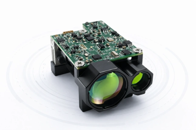
The laser driver and receiver share a PCB — 50 A nanosecond pulses operating 15 mm from picoamp-sensitivity analog circuits. Achieving >60 dB isolation between these domains is the defining PCB layout challenge in LiDAR design.
Isolation Strategies
- Physical Separation and Partitioning: Laser driver components on one end of the board, receiver components on the other. Minimum 15 mm separation between the two sections' component boundaries. Ground via fencing (ground vias on 1.0 mm pitch) along the boundary between sections, connecting all ground plane layers.
- Ground Plane Topology: Continuous ground plane on at least two internal layers. The laser driver's power return current must flow through the ground plane back to the bus capacitors — not through the receiver section's ground. This is achieved by ensuring the bus capacitors' ground connection is on the driver side of the via fence, so return current flows locally without crossing into receiver territory.
- Supply Domain Isolation: Separate voltage regulators for laser driver, receiver analog, receiver digital, and FPGA domains. Each domain's regulator output filtered with ferrite bead + ceramic capacitor. No shared plane copper between laser driver power and receiver power — separate pour areas connected only at the main power input.
- Timing of TX Blanking: The receiver is blanked (disabled or its gain reduced to zero) during the laser pulse and for a short time afterward (5–50 ns blanking window). The blanking control signal travels from the timing controller to the receiver — this trace must not couple the laser driver's switching transients into the receiver's sensitive front end. Route the blanking signal on an internal layer between ground planes, physically separated from both the laser driver and receiver analog paths.
Automotive and Industrial Qualification
Automotive LiDAR operates at -40°C to +105°C, survives 20 g shock and 5 g RMS random vibration, and must function for 15+ years — all while the laser remains eye-safe per IEC 60825-1 Class 1 at the system level.
Qualification Support
- IATF 16949 Manufacturing: HILPCB's automotive production follows APQP-defined control plans with Cpk ≥ 1.67 on critical parameters. PPAP Level 3 documentation for OEM qualification.
- Accelerated Reliability Testing: 1,000+ thermal cycles at -40°C/+125°C. High-Tg laminates (Tg ≥ 170°C) with CAF-resistant construction for long-term humidity exposure. Via reliability verified by IST (Interconnect Stress Testing) on qualification coupons.
- Conformal Coating: Automotive-grade acrylic or silicone coating (25–75 µm) protecting assembled boards from condensation, road salt spray, and cleaning chemicals encountered during vehicle assembly and wash processes.
- AEC-Q100 Component Support: HILPCB's component sourcing from authorized distributors ensures AEC-Q qualified components with full lot traceability for automotive product liability requirements.
Architecture-Specific PCB Considerations
- Mechanical Scanning LiDAR: Circular or sector-shaped PCBs fitting inside a spinning head. Signal transfer through slip ring or optical rotary joint — rigid-flex construction reduces connector count and improves reliability under continuous rotation at 10–20 Hz.
- Solid-State LiDAR (MEMS): Standard rectangular boards with tight MEMS mirror driver integration. High-voltage MEMS drive signals (80–200 V) coexisting with low-voltage electronics — creepage management between MEMS driver and digital control sections.
- Solid-State LiDAR (OPA): Optical phased array designs requiring ultra-precise phase control signals to hundreds of emitters. DAC outputs with sub-mV accuracy — analog routing discipline comparable to instrumentation-grade PCBs.
- Flash LiDAR: Single pulse illuminates entire scene — requires 2D detector array (SPAD or SiPM array) with per-pixel TDC. High-density HDI PCB construction for routing 128×128 or larger detector arrays to readout electronics.
Initiate your LiDAR PCB program with a DFM and isolation review →
Frequently Asked Questions
Why is loop inductance critical in a LiDAR laser driver PCB? A LiDAR laser driver switches currents of 5–50 A in as little as 2 ns. Any parasitic loop inductance (even a few nanohenries) will generate massive voltage spikes, which can exceed the absolute maximum ratings of the GaN FET or the laser diode and cause catastrophic failure.
How do you prevent laser driver noise from interfering with the LiDAR receiver? To achieve the necessary 60+ dB isolation, the laser driver and receiver circuits are physically separated by at least 15 mm on the PCB, partitioned by ground via fencing. Separate voltage regulators and isolated ground plane topologies ensure that the 50 A transmission pulses do not couple into the picoamp-sensitivity analog receiver path.
What materials are used for automotive LiDAR PCBs? Automotive LiDAR PCBs use high-Tg laminates (Tg ≥ 170°C) that resist Conductive Anodic Filament (CAF) growth under high humidity. These materials endure extreme temperature cycling (-40°C to +125°C) and meet the 15+ year operational lifespan required by automotive OEMs.
Can LiDAR PCBs support both solid-state and mechanical scanning architectures? Yes, HILPCB fabricates rigid boards for solid-state LiDAR (MEMS or Optical Phased Arrays), high-density HDI boards for Flash LiDAR detector arrays, and rigid-flex assemblies for spinning mechanical LiDAR to eliminate slip-ring connector complexity.