
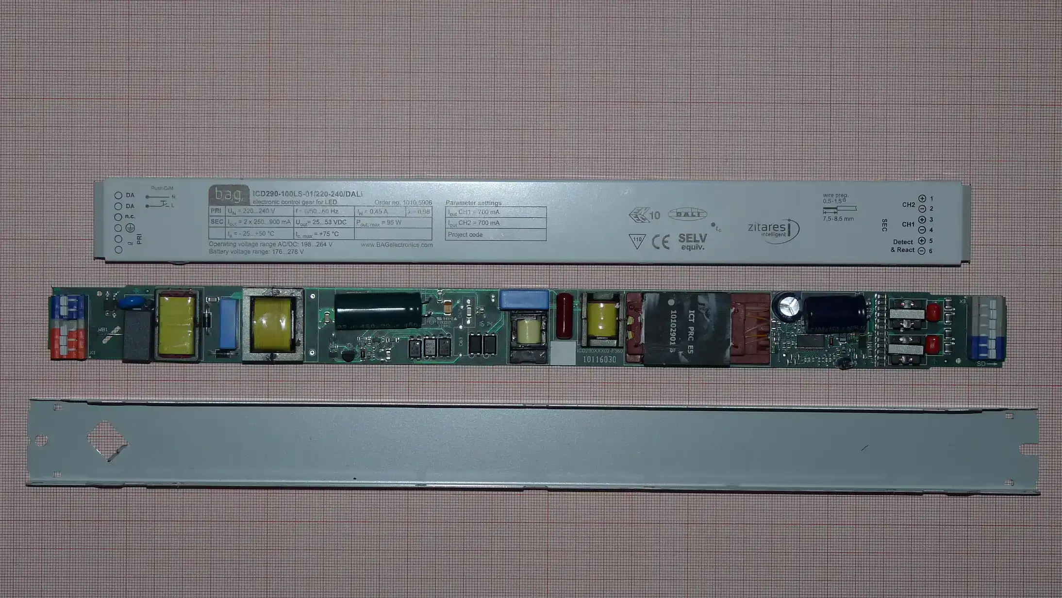
A linear LED driver PCB is often chosen when a lighting product needs a compact circuit, low component count, quiet electrical behavior, and predictable manufacturing cost. It is common in LED filament lamps, small decorative lamps, LED strips, low-power luminaires, appliance lighting, signage, and cost-sensitive products where the LED string voltage can be kept close to the supply voltage.
The design looks simple at first: regulate LED current by dropping excess voltage across a linear pass element or integrated linear driver IC. The real engineering challenge is less about schematic complexity and more about power loss, temperature rise, dimmer compatibility, safety spacing, LED placement quality, and batch-to-batch repeatability.
A good linear driver board should therefore be reviewed as both a power circuit and a thermal product. The PCB is not just a component carrier. It becomes part of the heat-spreading path, the LED optical layout, the dimming interface, and the manufacturing control plan.
Key takeaways
- A linear LED driver is best used when the voltage headroom between the supply and LED string is small enough that heat can be controlled.
- Linear drivers usually create less high-frequency EMI than switching drivers, but the finished luminaire still needs product-level EMC and safety validation.
- The main PCB risk is thermal: the excess voltage multiplied by LED current becomes heat inside the driver, LED substrate, and enclosure.
- Metal core PCB, high-thermal-conductivity dielectric, wide copper, thermal vias, and realistic enclosure testing matter more than headline driver simplicity.
- Phase-cut dimming compatibility depends on the whole system: dimmer type, holding current, bleeder path, input protection, LED load, and flicker behavior.
- PCB and PCBA test planning should include current regulation, ripple, thermal rise, dimming curve, polarity, optical binning, burn-in or aging, and traceability.
In this guide
- What a linear LED driver actually does
- When to choose a linear driver instead of a switching LED driver
- PCB thermal design for linear LED drivers
- Phase-cut, TRIAC, trailing-edge and flicker considerations
- MCPCB, ceramic, copper and FR-4 substrate choices
- Manufacturing, assembly and testing controls
- Common failure modes
- Cost drivers and RFQ checklist
- FAQ
What a linear LED driver actually does
A linear LED driver regulates current without using an inductor, transformer, or high-frequency switching power stage. In a simplified constant-current circuit, the LED string, current-sense path, and pass element are arranged so the driver adjusts its voltage drop to maintain the required LED current.
That operating principle is why the design can be compact. There are fewer magnetics, fewer switching-loop layout constraints, and fewer EMI-filtering parts than in a typical buck, boost, or buck-boost LED driver. For low-power lighting products with tight space limits, that simplicity can be very attractive.
The trade-off is direct and unavoidable. The driver dissipates the unused voltage as heat:
Power loss ≈ (Input voltage - LED string voltage) × LED current
If the LED string voltage is close to the input voltage, the wasted power may be manageable. If the voltage gap is large, the same circuit can become inefficient and thermally stressed very quickly. This is the central decision in every linear LED driver PCB review.
A linear driver can be a strong fit when the system has:
- a narrow input-voltage range
- a carefully matched LED string voltage
- moderate output current
- limited space for magnetics
- strong sensitivity to switching noise
- a cost target that does not justify a full switching supply
It is usually a weaker fit when the system requires wide input-voltage operation, high output power, high efficiency across many operating points, high power factor, or advanced digital control.
When to choose a linear driver instead of a switching LED driver
A switching LED driver transfers energy through a controlled switching node and an inductor, transformer, or coupled magnetic element. It is usually more efficient and more flexible over wide voltage ranges. A linear LED driver burns off voltage headroom as heat, but it is simpler and often quieter.
The best choice is not about which topology is “better.” It depends on voltage headroom, power level, dimming requirement, EMI budget, enclosure temperature, and product cost.
| Review item | Linear LED driver | Switching LED driver |
|---|---|---|
| Basic circuit structure | Simple current regulator or linear IC | Buck, boost, buck-boost, flyback, LLC or other switching topology |
| Efficiency behavior | Strongly depends on voltage headroom | Usually better over wide input/output conditions |
| EMI behavior | Lower switching-noise burden, but not automatically EMC-compliant | Requires careful switching-loop, filter and layout control |
| PCB size | Usually compact for low power | Larger when magnetics and EMI filters are included |
| Heat location | Driver IC/pass element and LED board can run hot | Heat spreads across switch, diode/MOSFET, inductor and control IC |
| BOM cost | Lower in simple applications | Higher, but often justified at higher power |
| Dimming fit | Can work well with selected phase-cut dimming designs | Better for advanced dimming, wide-range control and smart lighting |
| Best use cases | LED filament lamps, strips, decorative lamps, compact low-power lighting | High-power luminaires, wide-input drivers, industrial lighting, smart lighting |
The selection should be made with a thermal calculation, not only a cost comparison. A low-cost linear driver that overheats in the final enclosure will create more cost through rework, warranty risk, and shortened lifetime.
PCB thermal design for linear LED drivers
Thermal design is the most important part of a linear LED driver PCB. The board has to move heat away from the driver IC, current-sense resistor, LED packages, rectifier components, and protection parts while keeping the luminaire within its target temperature limits.
Start with the voltage-headroom calculation
Before layout, calculate worst-case driver dissipation across the real operating range:
| Condition | Why it matters | What to check |
|---|---|---|
| Maximum input voltage | Increases the voltage the linear driver must drop | Driver IC power loss, current-sense resistor stress and enclosure temperature |
| Minimum LED forward voltage | Increases excess voltage across the driver | LED bin tolerance, cold-start behavior and string matching |
| Maximum LED current | Directly increases heat | Current setting tolerance and dimming maximum |
| Highest ambient temperature | Reduces thermal margin | Thermal test in enclosure, not only open-air board test |
| Poor airflow or sealed lamp body | Traps heat around the PCB | Case temperature, solder-joint fatigue and LED lumen maintenance risk |
A practical design should test the hottest operating point with production-like LEDs, enclosure, lens, diffuser, thermal interface, and input supply. Open-bench thermal results can be misleading because the final lighting product often has limited airflow.
Use the PCB as a heat-spreading structure
For LED lighting, the PCB is part of the thermal path. HILPCB usually reviews these items first:
- Large copper areas under and around the driver IC and LED thermal pads.
- Thermal vias where the stackup supports vertical heat transfer.
- Metal core PCB when the LED board must move heat into an aluminum or copper base.
- High-thermal-conductivity dielectric for compact boards with higher LED density.
- Copper balance to reduce warpage during reflow.
- Solder-mask openings or defined thermal pads where the assembly needs better thermal interface contact.
For many LED boards, an MCPCB or high thermal conductivity PCB is more important than adding circuit complexity. A linear driver can be electrically simple, but it still needs a controlled thermal path.
Avoid turning one hot spot into a lifetime problem
Driver ICs, LEDs, rectifiers, and resistors should not be clustered without a thermal reason. In compact lamps, placing every heat source in the smallest area can raise local temperature enough to accelerate LED color shift, capacitor aging, solder fatigue, and polymer degradation.
A better layout spreads heat while preserving current-loop control. The goal is not only low peak temperature but also repeatable temperature distribution across production lots.
Phase-cut, TRIAC, trailing-edge and flicker considerations
Linear LED drivers are often used in retrofit or cost-sensitive lighting products that must work with existing dimmers. This can be convenient, but dimming compatibility is not automatic.
Phase-cut dimming is a system problem
A phase-cut dimmer changes the AC waveform delivered to the lamp. The driver input stage, rectifier, bleeder path, LED load, and current-regulation loop all influence whether the lamp dims smoothly or flickers.
| Dimming topic | Board-level concern | Risk if ignored |
|---|---|---|
| Leading-edge TRIAC dimming | Holding current, bleeder design, input surge and conduction angle | Flicker, dropout, audible noise or dimmer misfire |
| Trailing-edge dimming | Input capacitance, control-loop response and compatibility with electronic dimmers | Flashing, limited dimming range or unstable low-end behavior |
| Low-end dimming | Minimum LED current and driver dropout margin | Sudden turn-off, shimmer or inconsistent lamp-to-lamp behavior |
| Flicker | Current ripple and modulation depth | Visual discomfort, camera banding or product rejection |
| Surge and transients | Input protection and spacing | Damaged rectifier, driver IC or dimmer interface |
A TRIAC dimming PCB or trailing-edge PCB should therefore be tested with a representative set of dimmers, not with only one lab source. The PCB layout should also keep high-current rectifier and dimmer-interface currents away from sensitive sense nodes.
Flicker should be measured, not assumed
Linear drivers can respond quickly and can be very smooth in the right circuit. They can also show visible flicker if the rectified waveform, current regulation, capacitor sizing, or dimming circuit is poorly matched.
Flicker and modulation should be evaluated at full output, low dimming levels, warm and cold conditions, and across expected input voltage variation. IEEE 1789 is often referenced for LED flicker and modulation-frequency guidance, but the actual acceptance target should come from the product specification and target market.
MCPCB, ceramic, copper and FR-4 substrate choices
The substrate choice should follow the lighting product architecture. A low-power decorative lamp may not need the same material as a high-density LED module or a sealed outdoor luminaire.
| Substrate route | Where it fits | PCB design focus |
|---|---|---|
| Standard FR-4 | Low-power control board separated from LED heat | Cost, routing, basic creepage/clearance and assembly yield |
| High-Tg FR-4 | Driver boards exposed to elevated temperature | Dimensional stability and soldering robustness |
| Aluminum MCPCB | LED strips, modules, downlights, compact lamps | Thermal conductivity, dielectric thickness and isolation |
| Copper-base PCB | Higher heat flux or premium lighting modules | Lower thermal resistance and stronger heat spreading |
| Ceramic substrate | UV LED, high-power LED, laser light source, high-reliability modules | CTE match, thermal performance and cost control |
| Hybrid construction | Driver plus LED array with different thermal zones | Mechanical stackup, insulation and assembly sequence |
Surface finish also matters. ENIG can help with solderability and long storage windows, while OSP may fit cost-sensitive builds with tightly controlled assembly timing. For high-reflectance LED boards, solder-mask color, surface cleanliness, and LED placement accuracy can influence optical consistency.
EMI and safety boundaries
Linear LED drivers are often described as “EMI-free” because they do not create the same high-frequency switching node as a buck or flyback converter. That is too absolute for a finished product.
A linear driver can reduce switching-noise burden, but the luminaire can still have conducted emissions, surge issues, electrostatic discharge risks, phase-cut dimmer noise, rectifier current pulses, and cable-related radiation. PCB layout should still include:
- short input-current paths
- proper rectifier and bulk-capacitor placement
- protection near external connectors
- clean current-sense routing
- separation between live, neutral, SELV and user-accessible areas where applicable
- creepage and clearance rules based on operating voltage, pollution degree and product safety requirements
IEC 61347-2-13, IEC 62384, IEC 62368-1 or other standards may be relevant depending on the product category and market. The PCB can support the necessary spacing, thermal design, test access and traceability, but the finished driver or luminaire still needs product-level validation.
Manufacturing, assembly and testing controls
A linear LED driver PCB is often built in high volume, so repeatability matters. Small process changes can cause visible brightness differences, dimming inconsistency, or early failures.
PCB fabrication controls
For bare boards, HILPCB reviews:
- dielectric thickness and thermal conductivity for MCPCB
- solder-mask registration around LED pads
- copper thickness and current-carrying areas
- creepage/clearance around mains or high-voltage areas
- board flatness for LED placement and optical uniformity
- electrical test for opens and shorts
- finish selection based on shelf life and assembly process
LED PCBA controls
For assembly, the most important controls are paste volume, LED polarity, placement accuracy, thermal pad soldering, and optical bin management.
| Process step | What it verifies | Why it matters |
|---|---|---|
| SPI | Solder paste volume and shape | Prevents open joints, tombstoning and uneven LED thermal contact |
| SMT placement | LED polarity, position and rotation | Protects optical uniformity and avoids assembly scrap |
| Reflow profile | Solder wetting and thermal exposure | Prevents LED damage, cold joints and color drift from overheating |
| AOI | Missing parts, polarity, solder defects and contamination | Catches visual and placement defects before functional test |
| Electrical test | LED current, open/short, driver output and protection behavior | Confirms the board matches the circuit intent |
| Optical test | CCT, CRI, flux or brightness where required | Controls visible product consistency |
| Burn-in or aging | Early failure screening under powered conditions | Finds weak solder joints, bad LEDs or unstable drivers |
For dimmable products, testing should include full-output, low-output, turn-on, turn-off, and multiple dimmer conditions. For LED strips or modules, current uniformity along the length should also be checked.
Common failure modes
| Failure mode | Likely cause | PCB or PCBA prevention |
|---|---|---|
| Driver IC overheating | Excess voltage headroom, poor copper area, weak thermal path | Recalculate worst-case dissipation, enlarge copper, use MCPCB or higher thermal material |
| LED color shift or lumen drop | High junction temperature or poor LED thermal pad soldering | Improve thermal stack, verify solder coverage, test in final enclosure |
| Flicker at low dimming level | Poor phase-cut compatibility, insufficient holding current or unstable regulation | Test with representative dimmers, tune bleeder and input network |
| Random lamp dropout | Driver dropout margin too small or LED Vf variation too high | Review LED binning, string voltage, current setting and input range |
| Audible noise | Dimmer interaction, capacitor/ceramic vibration or mechanical resonance | Test dimming waveforms and component behavior in enclosure |
| EMI or surge failure | Inadequate input protection or uncontrolled current loops | Add protection, shorten loops, review spacing and grounding |
| Early solder-joint failure | Thermal cycling, board warpage or poor reflow profile | Control copper balance, material selection and reflow window |
| Uneven brightness | LED bin mixing, placement error or current imbalance | Manage LED bins, placement accuracy and functional/optical testing |
Cost drivers and RFQ checklist
Linear LED driver projects look simple, but pricing can vary significantly depending on substrate, finish, thermal target, assembly accuracy and testing requirements.
Main cost drivers
- MCPCB versus FR-4 or ceramic substrate
- dielectric thermal conductivity
- copper thickness and board thickness
- LED package type and placement tolerance
- surface finish and reflective solder mask
- dimming compatibility test scope
- optical binning and full or sampling optical test
- burn-in or aging time
- custom panelization and fixture requirements
- conformal coating or potting for harsh environments
What to send HILPCB for review
For a faster and more accurate quote, send:
- Gerber or ODB++ files
- schematic and BOM
- LED string voltage, current and power target
- input voltage range and dimming method
- driver IC datasheet or part number
- target substrate type, copper thickness and board thickness
- thermal target or maximum case temperature
- enclosure or heatsink information if available
- required surface finish and solder-mask color
- test requirements: electrical, optical, dimming, burn-in, aging or inspection reports
- production volume, prototype quantity and expected ramp schedule
Reference standards and design boundaries
The following standards can be relevant depending on the product market and final luminaire type. They should be treated as product or controlgear validation references, not as proof that a PCB alone is compliant.
- IEC 61347-2-13: Safety requirements for electronic controlgear for LED light sources.
- IEC 62384: Performance requirements for electronic controlgear for LED modules.
- IEEE 1789: Recommended practice related to LED modulation frequency and flicker risk.
- IEC 62368-1: Safety standard used for many audio/video, information and communication technology products where applicable.
- Regional EMC, energy-efficiency and lighting performance requirements as specified by the target market.
FAQ
Is a linear LED driver always less efficient than a switching LED driver?
Usually yes when the input voltage is much higher than the LED string voltage, because the extra voltage becomes heat. However, in low-dropout or closely matched LED-string designs, a linear driver can be efficient enough while staying simpler and cheaper than a switching solution.
Does a linear LED driver PCB have no EMI problem?
No. It may have much less high-frequency switching noise than a switching LED driver, but the complete luminaire can still have conducted noise, dimmer interaction, surge vulnerability, ESD issues and layout-related current-loop problems. Product-level EMC testing is still needed.
Why is thermal design so important for linear LED drivers?
Because the linear driver dissipates unused voltage as heat. If that heat is not moved into copper, MCPCB, housing or heatsink effectively, the driver and LEDs can run hot, causing brightness loss, color shift, unstable dimming or early failure.
When should I use MCPCB for a linear LED driver board?
Use MCPCB when the LED array or driver dissipates enough heat that standard FR-4 cannot maintain the target temperature in the final enclosure. Aluminum MCPCB is common for general LED modules, while copper or ceramic options may be used for higher heat flux or premium applications.
Can a linear LED driver support TRIAC or phase-cut dimming?
Yes, but compatibility depends on the dimmer, input network, holding current, LED load, bleeder design and current-regulation behavior. It should be validated with representative dimmers across the full dimming range.
What should be tested before mass production?
At minimum, test LED current, ripple, startup, dimming behavior, thermal rise, polarity, open/short faults and optical output. For higher-reliability lighting, add burn-in or aging, surge/ESD pre-checks, enclosure thermal testing and traceable inspection reports.
Conclusion
A linear LED driver PCB is a strong choice when the lighting product values simplicity, compact size, low BOM cost and low switching-noise burden. Its success depends on respecting the limits of the topology: voltage headroom becomes heat, dimming is a system-level interaction, and the PCB must provide a real thermal path rather than only an electrical connection.
HILPCB supports LED lighting teams with MCPCB, high-thermal-conductivity PCB, SMT assembly, dimming-board manufacturing, electrical testing and production traceability. Whether the project uses a simple linear constant-current driver, a TRIAC dimming PCB, a trailing-edge dimming board or a more complex switching LED driver, early review of stackup, substrate, thermal path and test requirements helps reduce re-spins and improves production stability.