HILPCB is a full-service PCB manufacturer with advanced capabilities in optical integration, photonic systems, and high-speed circuit board production. Our manufacturing and assembly solutions support a wide range of advanced applications, including optical PCBs for telecommunications infrastructure, medical instrumentation, industrial automation systems, and cutting-edge quantum computing platforms.
Beyond manufacturing, we provide end-to-end optical PCB assembly services, including precision placement of optical components, waveguide integration, VCSEL and photodetector mounting, and comprehensive testing with optical power measurement and signal integrity validation, ensuring optimal performance and long-term reliability for photonic transmission systems.
While our services span many industries beyond optical communications, our processes are perfectly suited for optical PCB assembly, integrated photonic systems, and other designs requiring precise optical alignment, waveguide integration, and seamless electronic-photonic convergence. From prototype to volume production, HILPCB ensures high-quality optical PCB delivery through consistent performance and rigorous process control.
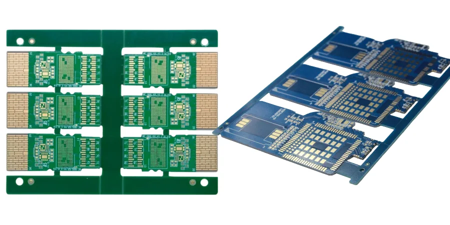
Advanced Optical PCB Design and Manufacturing Capabilities
Designing and producing optical circuit boards requires deep expertise in photonic integration, waveguide technology, and precision optical alignment. Our solutions support:
Integrated Waveguide Systems
Advanced polymer and glass waveguide fabrication with controlled refractive index profiles, supporting data rates up to 400 Gbps per channel with minimal optical loss and crosstalk for high-density optical interconnect applications.Multilayer and HDI PCB Integration
Our optical PCB stackups feature three-dimensional optical routing, precision alignment structures, and thermally stable substrates, ideal for compact photonic designs and high-density optoelectronic component integration.Professional Telecommunications Applications
From data center interconnects to 5G infrastructure, we manufacture precision optical PCBs meeting telecommunications industry standards, capable of handling extreme bandwidth requirements and electromagnetic interference immunity.Thermal-Optical Management
Advanced thermal control techniques including thermal isolation zones, temperature-compensated waveguides, and strategic component placement ensure wavelength stability and consistent optical performance across operating temperature ranges.
We also support hybrid optoelectronic systems, including designs that combine optical waveguides with high-speed electrical interfaces like PCIe, Ethernet, and proprietary protocols for comprehensive photonic-electronic convergence solutions.
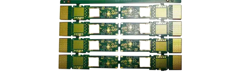
Advanced Optical PCB Manufacturing and Testing Processes
Our manufacturing workflow is optimized for optical PCB assembly, where optical alignment precision and photonic performance are critical:
Specialized Substrate Materials
We utilize high-frequency PCB materials with controlled optical properties, low birefringence, and stable thermal-optical coefficients across the entire wavelength spectrum required for telecommunications and medical applications.Precision Optical Component Assembly
Using advanced pick-and-place systems with active optical alignment, we mount VCSELs, photodetectors, and optical modulators with sub-micron positioning accuracy, ensuring optimal coupling efficiency and long-term reliability.Comprehensive Optical Testing and Validation
All optical PCBs undergo rigorous testing including insertion loss measurement, return loss analysis, optical power characterization, and wavelength stability validation to ensure compliance with industry optical specifications.Environmental Stress Screening
We simulate extreme conditions through temperature cycling (-40°C to +85°C), vibration testing, and humidity exposure to validate optical performance for aerospace, automotive, and industrial photonic applications.Optical Performance Certification
Our optical PCBs meet stringent telecommunications standards including ITU-T recommendations, IEC optical safety requirements, and automotive optical specifications for global deployment.
Optical PCB Applications Across Industries
We manufacture high-performance optical PCBs for diverse applications across multiple industries:
Telecommunications Infrastructure
5G/6G base stations, fiber optic transceivers, optical switches, submarine cable systems, data center interconnects, and high-speed optical networking equipment with advanced wavelength division multiplexing.Medical Device Systems
Endoscopic imaging systems, laser surgical platforms, optical coherence tomography equipment, photodynamic therapy devices, and wearable health monitoring systems with flex PCB integration.Industrial Automation Applications
Machine vision systems, LiDAR sensors, optical encoders, spectroscopic analyzers, factory automation networks, and robotic guidance systems requiring precise optical positioning and control.Automotive Photonic Systems
Autonomous vehicle LiDAR units, heads-up display systems, fiber optic communication networks, advanced driver assistance systems, and in-vehicle optical sensor networks with high-speed PCB technology.Quantum Computing Platforms
Quantum optical control systems, photonic quantum processors, quantum communication networks, cryogenic optical interfaces, and quantum sensing platforms requiring ultra-precise optical phase control.Defense and Aerospace Systems
Secure optical communication links, electro-optical targeting systems, satellite optical terminals, fiber optic gyroscopes, and ruggedized photonic systems with Rogers PCB materials.Research and Scientific Instrumentation
Optical spectrum analyzers, laser interferometry systems, particle detection equipment, optical microscopy platforms, and advanced photonic research instrumentation.Consumer Electronics Integration
AR/VR display systems, optical touch interfaces, 3D sensing cameras, high-speed optical storage systems, and advanced display technologies with integrated photonic components.Energy and Environmental Monitoring
Solar concentrator systems, optical power monitoring, environmental sensing networks, optical gas detection systems, and renewable energy optimization platforms.Data Center and Cloud Infrastructure
High-density optical interconnects, parallel optical modules, optical circuit switching systems, and advanced cooling monitoring with integrated photonic sensors.
We support custom optical PCB development for all applications, balancing optical performance requirements, cost constraints, and reliability expectations across mission-critical, commercial, and emerging photonic technology implementations.
Why Choose HILPCB as Your Optical PCB Manufacturing Partner
We go beyond standard PCB production to provide comprehensive support for your optical and photonic system development:
Specialized Photonic Design Expertise
Advanced waveguide design, optical alignment strategies, and thermal-optical optimization ensure optimal photonic performance and long-term stability with impedance calculator and optical modeling verification.Professional-Grade Manufacturing Standards
IPC Class 3, ISO 9001, and AS9100-based systems ensure complete traceability and industry-leading quality for telecommunications, medical, and aerospace photonic applications.Flexible Prototyping and Scalable Production
From initial development to long-term manufacturing, we support flexible batch sizes and on-time delivery to meet aggressive project schedules and market demands for optical system deployment.Expert Engineering Support
Optical system simulation, photonic compliance consulting, and thermal-optical analysis services optimize optical PCB performance and regulatory compliance for global markets.Complete Lifecycle Services
Including material procurement, SMT assembly, optical testing, design updates, and component obsolescence management for long-term optical system success.
Optical PCB Frequently Asked Questions
What is an optical PCB?
An optical PCB is a specialized circuit board that integrates optical waveguides and photonic components with traditional electronic circuitry. It enables high-speed optical signal transmission, wavelength division multiplexing, and seamless electronic-photonic integration for advanced communications and sensing applications.
Can HILPCB support medical-grade optical PCB applications?
Yes. We meet medical device standards including ISO 13485 quality systems, biocompatibility requirements, and enhanced safety protocols suitable for surgical equipment, diagnostic imaging systems, and implantable optical devices.
What makes optical PCBs different from traditional high-speed PCBs?
Optical PCBs integrate waveguide structures for light-based signal transmission, offering immunity to electromagnetic interference, higher bandwidth capacity, and lower power consumption compared to electrical interconnects. They require specialized materials and precision optical alignment during manufacturing.
Do you manufacture integrated photonic system PCBs?
Yes. We produce complete optical PCB assemblies with integrated lasers, photodetectors, optical modulators, and waveguide networks suitable for telecommunications, medical devices, and industrial automation applications.
Can I order both optical prototypes and production volumes?
Absolutely. We support complete lifecycle manufacturing from initial optical design validation to high-volume optical PCB production with consistent optical performance and delivery schedules.
What testing do you perform on optical PCBs?
Our comprehensive testing includes optical insertion loss measurement, return loss analysis, wavelength characterization, optical power verification, and environmental performance validation to ensure optimal photonic performance and specification compliance.
Do you support aerospace-grade optical PCBs?
Yes. We manufacture space-qualified optical PCBs meeting MIL-STD specifications with radiation-hardened components, extreme temperature cycling, and long-term reliability for satellite communications and defense applications.