
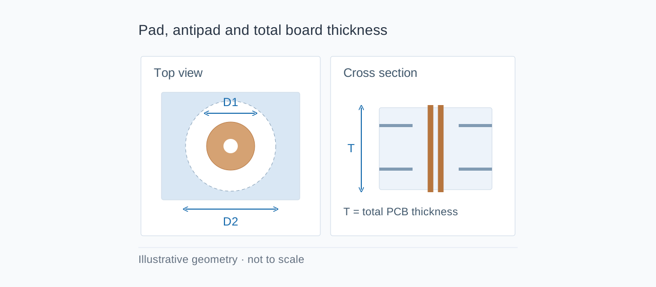
A via pad sits near copper in the reference planes and contributes parasitic capacitance. A simple approximation can show how pad diameter, antipad clearance and board thickness affect that estimate. It cannot replace a model of every plane, dielectric layer and return path in a real transition.
The PCB via capacitance calculator compares one geometry change at a time and plots ideal capacitive reactance against frequency. Begin by identifying the dimensions correctly: the hole, pad and antipad are different features.
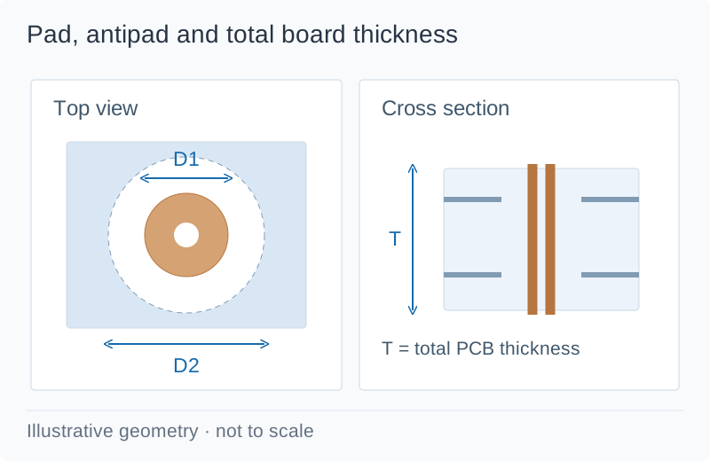
What are D1, D2 and T?
| Symbol | Meaning in this approximation | Common input mistake |
|---|---|---|
| D1 | Via pad diameter | Entering the drill or finished hole diameter |
| D2 | Clearance or antipad diameter in reference planes | Entering a radial clearance instead of a diameter |
| T | Total PCB thickness for the through-via approximation | Entering spacing to the nearest reference plane |
| εr | Assumed relative permittivity | Treating a generic laminate value as measured data at all frequencies |
The radial pad-to-antipad clearance is (D2 − D1)/2. A 0.60 mm pad inside a 1.00 mm antipad has a 0.20 mm radial clearance. The clearance diameter must exceed the pad diameter after any unit conversion.
T has a different meaning here from dielectric height in a microstrip impedance calculator. For the impedance workbench, the trace-to-reference geometry matters. For this particular through-via equation, T is the total PCB thickness. Moving the same number between the two tools without checking its definition changes the physical question.
Which formula does the calculator use?
Texas Instruments SLLA284G, Equation 1, printed page 15 gives the approximation. Expressed using millimetres:
C [pF] = (1.41 / 25.4) × εr × T [mm] × D1 / (D2 − D1)
The published coefficient uses inches; division by 25.4 converts T to the millimetre form. D1 and D2 must use the same unit, so their ratio remains dimensionless. The tool converts each input before evaluating the expression.
Plane count and hole diameter are not additional inputs to this equation. It is not a sum of individual parallel-plate capacitances, a blind-via model or a field solution. If you need to resolve separate plane spacings or an irregular clearance, choose a model that includes those features.
Worked example: a 1.6 mm through-via geometry
Set T = 1.60 mm, D1 = 0.60 mm, D2 = 1.00 mm, εr = 4.2 and evaluation frequency = 1000 MHz. The calculator returns C = 0.559559 pF. The table changes one dimension per row:
| Case | T | D1 | D2 | Estimated C | Change | Ideal magnitude of Xc at 1 GHz |
|---|---|---|---|---|---|---|
| Baseline | 1.60 mm | 0.60 mm | 1.00 mm | 0.559559 pF | — | 284.429 Ω |
| Antipad 25% larger | 1.60 mm | 0.60 mm | 1.25 mm | 0.344344 pF | −38.46% | 462.197 Ω |
| Pad 25% smaller | 1.60 mm | 0.45 mm | 1.00 mm | 0.305214 pF | −45.45% | 521.454 Ω |
| Board 25% thinner | 1.20 mm | 0.60 mm | 1.00 mm | 0.419669 pF | −25.00% | 379.239 Ω |
These alternatives show mathematical sensitivity. A smaller pad still needs sufficient annular ring and registration allowance. A larger antipad removes more reference-plane copper and can affect return-current continuity or nearby structures. A thinner board changes mechanical and stackup constraints. None of the rows is an automatic manufacturing recommendation.
Why are small clearances sensitive?
The denominator D2 − D1 becomes small as the two diameters approach one another. Keep T, D1 and εr at the baseline values but reduce D2 from 1.00 to 0.65 mm. The estimated C becomes 4.47647 pF, eight times the baseline because the diameter difference falls from 0.40 to 0.05 mm.
That sharp change explains why dimensional tolerances matter. It does not prove the approximation remains accurate as the gap tends to zero. D2 = D1 is undefined, and D2 < D1 is invalid for this geometry. A negative capacitance from that input combination is an input/model error rather than a usable result.
Does frequency change capacitance?
Not in this constant-permittivity geometry model. Frequency changes ideal capacitive reactance magnitude:
|Xc| [Ω] = 10⁶ / {2π × f [MHz] × C [pF]}
The baseline gives about 2844.29 Ω at 100 MHz and 284.429 Ω at 1 GHz. At DC an ideal capacitor is an open circuit. The tool shows that state rather than a finite number; it does not calculate dielectric leakage.
A smaller capacitive reactance magnitude is not the same as a smaller series resistance. Its effect depends on how the capacitance connects into the transition. The plotted curve does not predict insertion loss, resonance or usable bandwidth. Real material permittivity and loss can also vary with frequency.
How should you use the result in a design review?
Record the exact pad/antipad definitions, total thickness, material assumption and the transition being compared. Use the tool to identify which dimension deserves a tolerance study. Then review the complete structure, including layer-specific pads and clearances, barrel length, unused stub and reference planes.
Read the companion via inductance guide to understand the separate barrel estimate. Do not turn the two standalone outputs into a claimed resonance using an ideal LC equation: they do not describe all the distributed effects of a real via transition.
FAQ
Is the antipad the same as the hole diameter?
No. The antipad is a copper clearance in a reference plane. The hole is the drilled or finished opening through the board. D2 in this calculator is the antipad diameter.
Should T be the distance to the closest plane?
No. This TI through-via approximation uses total PCB thickness. A model based on individual plane distances is a different calculation.
Does a larger antipad always improve the design?
It lowers this capacitance estimate when the other inputs remain fixed. It can also alter return continuity and surrounding copper. Review the entire transition and fabrication constraints.
Can this calculate a blind microvia's capacitance?
It implements the stated through-via approximation. Use a model matched to blind-via geometry and its actual reference planes for that purpose.
Compare pad and antipad dimensions before requesting a stackup and fabrication review.