
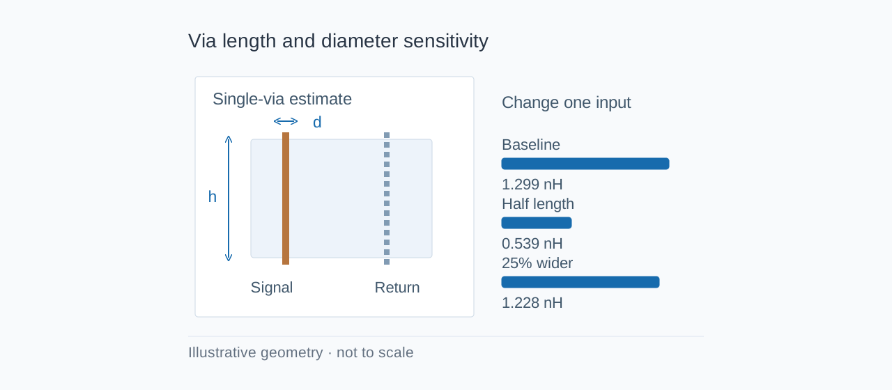
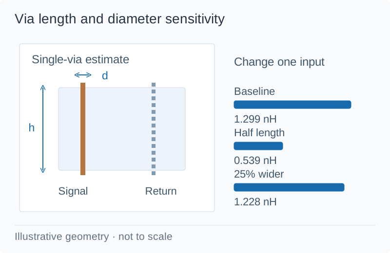
A via contributes inductance even when its DC resistance is small. For a first geometry comparison, reducing barrel length usually changes the estimate more strongly than a modest diameter increase. The return path remains essential: a single-via calculation cannot determine the inductance of the complete signal or power loop.
Use the PCB via inductance calculator to compare dimensions and inspect ideal inductive reactance versus frequency. Keep the geometry estimate separate from the insertion loss or bandwidth of a complete transition.
What does the via inductance formula calculate?
The tool implements the single-via approximation in Texas Instruments SLLA284G, Equation 2, printed page 16:
L [nH] = 0.2 × h [mm] × {ln[4h/d] + 1}
Here h is the modeled via length and d is the via diameter. Use the same length unit inside the logarithm and the natural logarithm, ln. The 0.2 coefficient above is for h in millimetres and L in nanohenries. The diameter d is not the pad or antipad diameter.
The calculator screens geometry to h ≥ d and dimensions from 0.01 to 100 mm. That is an application screen to avoid unsuitable shapes, not a published guarantee of accuracy throughout the range. A short, wide interconnect needs an appropriate field model rather than forcing it through this equation.
This approximation does not include a nearby return conductor, plane coupling, mutual inductance between vias, pad capacitance or a stub resonance. Selecting h should describe the segment you are evaluating; editing h does not automatically model the rest of a partially used through via.
Worked example: shorten the via or enlarge its diameter?
Set h = 1.60 mm, d = 0.30 mm and frequency = 1000 MHz. Change one dimension at a time:
| Geometry | Length h | Diameter d | Estimated L | Change in L | Ideal XL at 1 GHz |
|---|---|---|---|---|---|
| Baseline | 1.60 mm | 0.30 mm | 1.29929 nH | — | 8.16366 Ω |
| 25% shorter | 1.20 mm | 0.30 mm | 0.905421 nH | −30.31% | 5.68893 Ω |
| 50% shorter | 0.80 mm | 0.30 mm | 0.538740 nH | −58.54% | 3.38500 Ω |
| 25% wider diameter | 1.60 mm | 0.375 mm | 1.22788 nH | −5.50% | 7.71500 Ω |
The difference follows from the equation: length multiplies the entire expression and also appears inside the logarithm. Diameter appears only inside the logarithm. These results support a geometry comparison for this example; they do not imply that every design should use a thinner board or a larger drill.
A wider hole also changes annular-ring requirements, routing space and fabrication constraints. A shorter barrel can require another layer assignment or a different via construction. Compare those consequences with the impedance and stackup workbench before changing the design.
Why does frequency change reactance but not this inductance?
The geometry-only approximation returns the same L at every evaluation frequency. Ideal inductive reactance is:
XL [Ω] = 2π × f [MHz] × L [nH] × 0.001
For the baseline 1.29929 nH, XL is about 0.816366 Ω at 100 MHz and 8.16366 Ω at 1 GHz. At DC its ideal reactance is zero, but the real barrel still has copper resistance. The via current calculator handles that separate DC resistance estimate.
An 8.16 Ω reactance is not an 8.16 Ω resistance and does not mean the transition dissipates power like an 8.16 Ω resistor. It also does not directly specify reflection or insertion loss without the surrounding circuit and return structure.
Should you enter clock frequency or rise time?
Fast edges contain frequency content above the clock repetition rate. A 25 MHz clock with a 1 ns edge should not be assessed only at 25 MHz.
The tool's rise-time mode uses feval [MHz] = 350 / tr [ns]. A 1 ns edge therefore selects 350 MHz and gives about 2.85728 Ω for the baseline geometry. This is the 0.35/tr bandwidth estimate for a single-pole 10–90% rise-time convention. It is not the highest harmonic of every waveform or a complete channel specification.
Record whether the rise time is measured, simulated or specified, along with its measurement definition and loading. Use the actual driver and receiver models when the transition can affect a timing or signal-integrity margin.
What does a nearby return via change?
A signal changing reference planes needs a suitable return-current path between those references. Moving the return path far away can enlarge the current loop even if the signal barrel dimensions stay unchanged. A nearby ground return via can help when it connects the relevant ground references, but its effect depends on spacing and the complete stackup.
The single-via formula does not change when you move that return via because return geometry is absent from its inputs. Do not divide its L by the number of parallel vias to claim a loop-inductance result: mutual coupling and current distribution matter.
For a critical transition, model the signal via, pads, antipads, connected traces, reference planes, return conductors and unused stub together. Correlate the model with the measurement appropriate to the project. TI's High-Speed Layout Guidelines provide further layout context.
FAQ
Does doubling via diameter halve its inductance?
No. Diameter enters a logarithm in this approximation. For the stated baseline, a 25% increase reduces the estimate by about 5.50%.
Can I use the result as the complete loop inductance?
No. Return geometry and mutual coupling are absent. Use a loop or field model that includes the actual current path.
Does a lower inductance prove better high-speed performance?
It can be useful, but capacitance, impedance discontinuities, stubs, loss and return continuity also matter. A lower isolated L does not prove a better complete channel.
Can I combine the inductance and capacitance calculators to find a via resonance?
They provide separate geometry approximations. Substituting their outputs into an ideal LC equation does not establish the resonance or usable bandwidth of a distributed multilayer transition.
Explore the length and diameter comparison and read the companion via capacitance guide before reviewing the complete transition.