
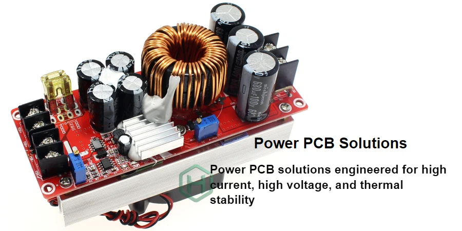
Power electronics used in power supplies, inverters, motor drives, and energy systems place very different demands on a PCB than signal-level designs. High current paths must minimize resistance and temperature rise, thermal hotspots must be engineered out at the layout and stackup level, and high-voltage sections must maintain safe creepage/clearance to prevent insulation breakdown. Delivering stable performance at scale requires the right heavy copper process controls, repeatable lamination/plating, and assembly practices tuned for power components.
At HILPCB, we provide end-to-end high current PCB solutions: thick copper fabrication (commonly 2–20 oz where appropriate), thermal management planning, and reliable power PCB assembly service for high-current and high-reliability products. From prototype validation to volume production, our engineering support focuses on manufacturability, consistency, and practical cost control for PCB for power electronics.
High Current Distribution with Heavy Copper Power PCBs
High current causes copper loss (I²R), voltage drop, and heating. Heavy copper layers (commonly 2–10 oz depending on design needs) reduce resistance and increase current capacity, but they also impact etching tolerance, spacing, and assembly thermal profiles. A manufacturable power PCB balances copper weight, geometry, and process capability.
Key Heavy Copper Design Practices
- Trace/Plane Sizing by Temperature Rise: Size copper based on allowable temperature rise and airflow/heat sinking—not only current. This improves reliability and prevents conservative oversizing that drives cost.
- Copper Weight Selection by Function: Use thicker copper on power layers and keep signal/control layers at standard copper where possible. This improves manufacturability and cost while protecting performance.
- Parallel Paths and Plane Architecture: Prefer planes and short, wide paths for high current loops to reduce inductance and voltage drop, especially in switching stages.
- Via Current Sharing: Use multiple vias (or via arrays) when moving current between layers. Current-sharing prevents localized heating and improves robustness.
- Terminations for High Current Interfaces: Design land patterns for screw terminals, press-fit pins, or high-current connectors with sufficient annular ring and copper support for mechanical and electrical reliability.
- Busbar Strategy When Needed: For extreme currents, a PCB can act as the control and interconnect platform while a busbar carries the primary current—often the most stable and economical approach.
Manufacturing and Verification
For production power PCBs, consistent copper thickness and plating uniformity matter as much as nominal oz. HILPCB supports these builds with DFM review and process controls so the delivered current-carrying capacity matches the design intent across batches.
Thermal Management for Power Components and Copper Planes
Power semiconductors, magnetics, and copper losses create concentrated heat. Thermal design is not a single feature—it is a system that includes copper spreading, thermal vias, heat sink interfaces, and assembly materials.
Key Thermal Management Techniques
- Thermal Via Arrays Under Hot Devices: Dense thermal vias under MOSFETs/IGBTs/rectifiers move heat into inner planes or backside heat spreaders.
- Copper Spreading and Heat Distribution: Use large copper areas on appropriate layers to reduce hotspots and stabilize temperature gradients.
- Heat Sink and Interface Planning: Define mounting points, keep-out zones, and TIM contact areas early so the mechanical and PCB designs match.
- Material Choice for Temperature Stability: For elevated operating conditions, select materials such as high-Tg PCB to maintain stability and reliability.
- Component Placement for Thermal Separation: Separate the hottest components and align them with airflow/cold plate zones to avoid thermal stacking.
- Assembly Profile Control: Reflow profiles and solder selection must match the thermal mass of heavy copper boards to maintain yield and joint quality.
Thermal Validation
Thermal simulation and IR measurement at realistic load conditions confirm the design margin. For power products, validating both steady-state and transient thermal behavior is often the difference between a good prototype and a stable production design.
High-Voltage Isolation: Creepage, Clearance, and Safety Margins
Many power products combine high current with high voltage. Electrical safety depends on correct creepage/clearance design, board geometry, and insulation strategy aligned with your target standard and pollution degree/environment.
Key Electrical Isolation Techniques
- Creepage/Clearance Planning: Define rules early based on your working voltage, environment, and safety standard requirements, then lock them into layout constraints.
- Isolation Barriers and Partitioning: Physically separate HV and LV areas and avoid routing that accidentally reduces clearance through copper pours or test pads.
- Slots and Cutouts for Added Margin: Milled slots can increase creepage distance and improve safety margin in compact designs.
- Surface Protection Where Needed: Conformal coating or potting can support environmental robustness, but it should not be used as a substitute for correct spacing.
- Hi-Pot and Insulation Testing: Production testing (as applicable to the product category) confirms process stability and helps prevent early-life failures.
Documentation for Compliance
Well-defined drawings, stackup notes, and manufacturing test requirements make compliance smoother for power products that must pass customer audits or certification processes.
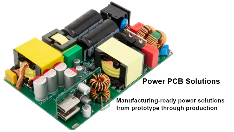
EMI Control for Switching Power Supplies and Inverters
Switching edges and loop inductance drive EMI. PCB layout is one of the most effective EMI tools—often more impactful than “adding filters later.” Managing loop area, return paths, and grounding strategy improves both emissions and functional stability.
Practical EMI Layout Approaches
- Minimize High di/dt Loop Area: Keep switch-node loops short and compact; place critical parts close (FET, diode, input caps, snubbers).
- Ground Return Discipline: Provide clean, low-impedance return paths and avoid routing that forces return current detours.
- Gate Drive Layout Optimization: Reduce gate loop inductance to control ringing and avoid unnecessary overshoot.
- Snubber and Damping Networks: Reserve placement space for RC/RCD snubbers and damping so you can tune during validation.
- Filter Placement Strategy: Put input/output filter components where they intercept noise effectively (not “wherever there’s room”).
- Segregate Power and Control Zones: Clear partitioning simplifies grounding and reduces coupling into sensing and control circuits.
EMI Validation Support
Power EMI is usually iterative. A manufacturable PCB with reserved tuning options accelerates pre-compliance testing and reduces redesign cycles.
Cost-Optimized Power PCB Manufacturing Without Over-Spec
Heavy copper, special materials, and added processes can raise cost quickly. The goal is to meet electrical and thermal requirements with the simplest reliable construction.
Cost Optimization Strategies
- Selective Heavy Copper Usage: Apply thick copper only where current demands it; keep other layers standard.
- Right-Sized Copper Weight: Choose copper weight from current + temperature rise requirements rather than using maximum thickness by default.
- Avoid Unnecessary Complex Processes: Use standard vias, standard finishes, and standard stackups where possible to improve yield.
- Panel Utilization Planning: Efficient panelization reduces material waste and improves throughput.
- Early DFM Collaboration: A short design review can eliminate high-cost features before they become locked into the design.
Total Value Perspective
A stable process and strong yield often reduce total cost more than small unit-price savings. Reliable power PCBs minimize rework, field returns, and performance variability.
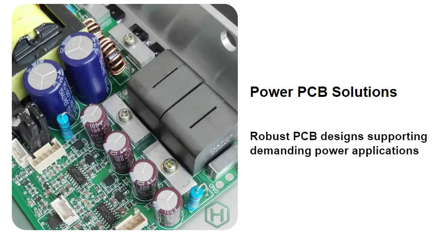
Fast Prototype Builds for Power PCBs and High-Current Validation
Power hardware development requires fast iteration because thermal, EMI, and current distribution interact. Prototype builds should match production intent so validation results translate.
Prototype Service Highlights
- Quick-Turn Heavy Copper Builds: Common heavy copper configurations can be prototyped quickly when stackups and materials are selected early.
- Power-Focused DFM Checks: Review current paths, via arrays, thermal features, and HV spacing before fabrication.
- Assembly Integration: For functional validation, combining fabrication + power PCB assembly service shortens the path to tested hardware.
- Targeted Verification: Thermal imaging, current stress checks, and basic electrical testing help confirm margins before scaling.
Faster Learning Cycles
Reducing prototype turnaround time speeds up tuning for EMI/thermal performance and helps lock a manufacturable design sooner.
Power PCB Applications: Inverters, Motor Drives, and Power Supplies
Power PCBs are used across many domains, and each has different priorities (efficiency, size, safety, ruggedness, or EMI).
Typical Application Areas
- Power Supplies: AC-DC and DC-DC designs demanding compact switching layouts, stable control loops, and repeatable assembly.
- Inverters: Renewable energy and industrial inverters needing strong current distribution, thermal planning, and EMI control.
- Motor Drives: VFDs and servo drives requiring robust power stages, protection circuits, and noise-resistant sensing.
- Battery Systems: BMS and power distribution boards that prioritize reliability, thermal stability, and safe isolation.
- Industrial and Automotive Power Electronics: Designs where long service life, harsh environments, and compliance requirements drive the build approach.
Conclusion
A reliable Power PCB is the result of coordinated current distribution, thermal engineering, high-voltage safety design, and EMI-aware layout—backed by manufacturing processes that hold tolerance consistently in production. HILPCB supports power electronics teams with heavy copper fabrication, practical DFM guidance, and scalable power PCB assembly service to help prototypes translate smoothly into volume builds.
If your roadmap also includes high-speed interconnect projects, you can reference our HDMI PCB manufacturing guide for fabrication and assembly considerations around controlled impedance and connector-focused layout.
Contact HILPCB for high current PCB solutions, prototype builds, or volume production support—optimized for manufacturability, stability, and long-term reliability.
Common Questions
What makes a power PCB different from a standard control board?
Power boards are driven by current distribution, thermal management, high-voltage spacing, and EMI coupling constraints much more than ordinary signal boards. Their layout and process window are usually tighter because electrical stress is higher.
Why should a power PCB prototype stay close to the production build?
If the prototype uses different copper weight, stackup, isolation distance, or assembly approach, its thermal, efficiency, and EMI results will not translate well into production. A production-like prototype gives more trustworthy design decisions.
Which applications usually need heavy copper or stronger isolation?
Inverters, motor drives, BMS hardware, power modules, and high-voltage conversion equipment are common examples. These products often face current surges, temperature rise, and safety compliance at the same time.