
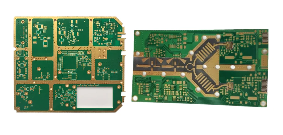
Rogers 4350B PCB builds can reduce dielectric loss relative to a selected FR-4 construction. Review RO4350B cores, copper, bonding layers, impedance targets and test requirements together; neither FR-4 nor PTFE is automatically unsuitable. Drilling, lamination and hybrid RF/digital stackups require review against the actual materials, geometry and acceptance plan.
RO4350B is an option for RF and microwave circuits when modeled and measured loss, phase and temperature behavior meet the application. A laminate name alone does not establish a usable frequency ceiling or a factory’s qualified RF test range.
RO4350B is a woven-glass-reinforced hydrocarbon/ceramic thermoset RF laminate. The standard RO4000 datasheet distinguishes process Dk 3.48 ± 0.05 at 10 GHz/23°C by clamped stripline from design Dk 3.66 by differential phase length over 8–40 GHz. Typical Df is 0.0037 at 10 GHz/23°C. The 4 mil thickness lists process Dk 3.33 ± 0.05; use the exact thickness and copper construction notes rather than treating these values as interchangeable.
Rogers 4350B PCB vs Standard High-Frequency Laminates
RO4350B can be a useful compromise among loss, cost and FR-4-compatible processing, but suitability for 5G or 77–81 GHz radar must be demonstrated against the actual trace geometry, launch design and insertion-loss budget. RO3003 and other RF materials are alternatives when the measured channel requirements favor them.
| Property | Rogers 4350B PCB | RO3003 | RO4003C | FR-4 |
|---|---|---|---|---|
| Process Dk at the published 10 GHz test basis | 3.48 ± 0.05 (process) | 3.00 ± 0.04 | 3.38 ± 0.05 | Grade/construction dependent |
| Df @ 10 GHz | 0.0037 | 0.0010 | 0.0027 | Grade/frequency dependent |
| Process family | Hydrocarbon ceramic (FR-4-like) | PTFE ceramic | Hydrocarbon ceramic | Epoxy glass |
| Hole preparation | Inspect smear; qualify the complete stackup | PTFE-specific preparation required | Inspect smear; qualify the complete stackup | Qualify resin desmear and metallization |
| Selection consideration | Loss, flame rating and processing | Low-loss PTFE construction and processing | Loss and application acceptance | Exact grade and channel loss budget |
Rogers’ 2025 selector notes a nominal process Dk of 3.04 for 0.060-inch RO3003/RO3203 under IPC-TM-2.5.5.5 because fixture air-gap bias is eliminated. Use the thickness-specific value and method.
RO4003C/RO4350B values above are typical process/test values, not finished-board acceptance limits. Use each material’s specified test method and a frequency-appropriate model; the generic FR-4 column is not a single laminate specification.
Rogers 4350B Material Engineering and Electrical Characteristics
RO4350B has published dielectric and thermal properties measured under specified methods. Its typical X/Y/Z CTE values and design Dk are useful starting points; frequency- and temperature-dependent behavior must be checked against the relevant datasheet and material thickness.
RO4350B is compatible with lead-free processing when lamination and assembly profiles are qualified for the stackup and components. Its published thermal conductivity is about 0.69 W/(m·K) at 80°C by ASTM C518; moisture absorption is test-method- and thickness-dependent, so neither figure alone guarantees outdoor lifetime.
Glass weave, conductor profile, line geometry and dielectric anisotropy can influence loss and skew. Specify the copper roughness and material model relevant to the intended RF frequency, then validate with suitable line coupons.
Advanced Rogers 4350B Fabrication Processes and Manufacturing Controls
HILPCB supports RO4350B special fabrication, hybrid-stackup review, drilling, lamination and plating. Qualified construction options include a 10:1 plated-hole aspect ratio, ±0.05 mm backdrill, ±0.03 mm 0201 placement and ±0.025 mm flip-chip placement; engineering can also provide 3D electromagnetic field solving. Calibrated VNA return-loss, insertion-loss and group-delay measurements, plus reviewed RF testing up to 110 GHz, can be scoped with documentation, traceability, consultation and assembly. These are build- and test-site-specific options, not blanket DC–40 GHz factory qualification.
Choose drill tooling, speed, chip load, entry/backup and tool life for the hole diameter, copper and complete stackup. Inspect hole walls and microsections to qualify plating and interconnect quality; one proprietary drill-angle/feed recipe does not establish capability for every construction.
RO4350B processing uses laminate- and stackup-approved lamination profiles. Temperature, pressure, dwell time and cooling rate must follow the fabrication method and material supplier guidance; a single 370°C/350 psi recipe is not a general requirement.
RO4000 materials do not require the PTFE-specific sodium treatment used for some PTFE laminates. Determine desmear from the drilled hole walls and bonding material; qualified chemical or plasma processing may be appropriate. Agree cleaning, copper preparation and metallization conditions for the construction rather than imposing one plasma power or a universal via aspect ratio.
Controlled Impedance Engineering for Rogers 4350B Applications
For a 50 Ω RO4350B microstrip, calculate line width from the dielectric thickness, process/design Dk assumption, final copper geometry and reference-plane environment. Verify modeled impedance against a suitable coupon rather than relying on one fixed width for all 0.508 mm laminates.
Stripline impedance depends on plane-to-plane spacing, conductor thickness and width, resin/laminate construction and copper roughness. A field solver and manufacturing coupon are needed to validate a proposed 50 Ω geometry.
Differential impedance and skew for edge- or broadside-coupled pairs depend on the full stackup. Solve the actual dimensions and tolerances, then validate the fabricated geometry and relevant interface limits.

Rogers 4350B Layer Stackup Optimization and Via Architecture
Multilayer configurations can place RO4350B on critical RF layers and compatible FR-4 on other layers. Specify the exact cores, bondply/prepreg, copper balance and final dielectric thicknesses. Hybrid compatibility, resin fill, registration and thermal history must be qualified; there is no universal 10-layer arrangement or guaranteed saving.
Laser microvias require a qualified buildup dielectric, copper opening and geometry; the RO4350B core label alone does not establish laser-process suitability. Back-drilling can shorten unused through-via stubs. Specify residual stub, depth tolerance, keepout and inspection against the actual layer positions, and validate the remaining transition rather than assuming all resonances disappear.
For blind/buried structures, define the sequential drilling, plating, bonding and inspection route for the actual interconnects. Verify cumulative thermal exposure and registration; not every multilayer needs sequential lamination or an identical subassembly process.
High-Power Rogers 4350B Thermal Management and Assembly Optimization
Thermal via arrays can spread heat between copper layers, but their effectiveness depends on plating, via pitch, pad construction and the connection to an external heat sink. Junction-to-case thermal resistance is primarily a package metric, not a fixed PCB via percentage improvement.
Use a reflow profile approved for the solder alloy, components, laminate and assembled board. Peak temperature and heating/cooling ramps must come from those constraints and process validation, not a generic RO4350B value.
Component placement and solder-joint acceptance should follow actual package pitches, stencil geometry, process capability and inspection criteria. Any claimed positional tolerances require measured production records.
Rogers 4350B Quality Assurance and Advanced Testing Protocols
RO4350B material identity and dielectric performance should be supported by the supplier datasheet, lot records and appropriate measurement methods. A finished-board impedance coupon does not independently determine bulk Dk; avoid unverified ±1% RF metrology claims.
For RF acceptance, agree calibrated VNA measurements, frequency range, fixtures, reference planes and de-embedding. Return loss, insertion loss and group delay requirements belong to the actual network; confirm the responsible test provider and reports rather than inferring available instruments from a service label.
Select environmental qualification methods from the actual automotive, aerospace or other customer program. Define sample construction, cycle temperatures, dwell, acceptance and failure analysis under the applicable test standard; an unspecified “modified IPC” test does not establish qualification or lifetime.
Advanced Rogers 4350B Applications and Industry Solutions
Automotive radar at 77–81 GHz requires a demonstrated antenna/feed loss and phase budget. RO4350B may suit some constructions, while other low-loss grades may be preferable. For turnkey assembly, specify the RF test frequency, fixture and acceptance plan and confirm the responsible laboratory.
RO4350B is used in some beamforming and RF front-end constructions, but phase matching is a design-specific requirement. Quote phase balance only after modeling and measuring the antenna/feed network across relevant temperature and frequency conditions.
For satellite and space-facing applications, verify outgassing, radiation, vacuum, thermal-cycling and documentation requirements for the complete material and assembly. An RF laminate does not receive automatic space qualification merely because it serves a Ka-band design.
Cost-Effective Rogers 4350B Manufacturing Strategies and Supply Chain Optimization
Rogers 4350B material costs can be optimized through intelligent panel utilization and hybrid stackup strategies. Mixed material designs utilizing Rogers 4350B only for performance-critical layers can reduce material usage, but savings and RF performance require quote-based cost and prototype verification. Our design optimization services identify cost reduction opportunities without compromising performance requirements.
For small batch assembly, confirm exact laminate/copper availability, panel utilization, tooling, test fixtures and minimum purchase quantities. Compare prototype and volume quotes for the same acceptance scope; stocking and lead time are build-specific commitments.
Rogers 4350B availability, copper option, lot evidence, and procurement lead time must be confirmed for each build. The purchase specification should also define incoming checks and the traceability documents required through fabrication. These confirmations are limited to the quoted construction and its supporting records.
Prepare a Rogers 4350B Manufacturing Review
Provide released RF geometry, stackup, exact RO4350B thickness/copper, bonding materials, via structure, assembly constraints and required electrical/environmental evidence. Confirm fabrication and external test responsibilities, material traceability and acceptance coupons before release. Compare measured channel performance and the quoted manufacturing route against the application requirements.