
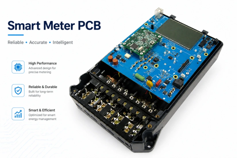
Over 1.3 billion smart meters will be deployed globally by 2028. Each one runs continuously for 15–20 years on a pole, in a meter box, or embedded in a wall — surviving -40°C to +70°C temperature swings, humidity approaching condensation, voltage transients from lightning coupling through the distribution network, and consumers physically attacking the meter with magnets, bypassing terminals, or drilling through the case to access the PCB.
The board must maintain Class 0.5S revenue-grade accuracy (±0.5% across the full current range from 50 mA starting current to 100 A maximum) over that entire service life without recalibration. It simultaneously manages PLC or RF communication with the utility's head-end system, detects and logs tamper events with tamper-proof timestamps, and survives 6 kV impulse withstand testing on the mains terminals.
Consumer electronics target 3–5 year life. Smart meters must function flawlessly for 20 years in uncontrolled environments. Every material selection, component derating choice, and manufacturing process decision reflects this fundamental difference. HILPCB manufactures smart meter PCBs for utility meter OEMs worldwide, from pilot deployments through 100,000+/year volume production with IPC-6012 Class 2/3 fabrication and full lot traceability.
Menu Navigation
- Metrology Front End: Achieving 0.1% Channel Accuracy
- Communication Stack: RF, PLC, and Cellular
- Anti-Tamper Hardware Design
- High-Voltage Isolation Under IEC 62052/62053
- 20-Year Reliability Engineering
- Manufacturing for Utility-Scale Deployment
Metrology Front End: Achieving 0.1% Channel Accuracy
The metrology subsystem measures voltage and current through shunt resistors or current transformers, feeds the resulting analog signals into a dedicated metering IC or metrology-grade sigma-delta ADC, and computes active, reactive, and apparent power, energy accumulation, power factor, and harmonic content. The PCB layout directly determines whether the assembled meter achieves and maintains Class 0.5S accuracy.
Analog Front End Layout
- Kelvin Connections on Current Shunts: For shunt-based single-phase meters, sense traces from the shunt resistor (typically 100–300 µΩ manganese copper alloy) must route directly to the metering IC's differential current inputs. The sense traces must not share copper with the power path carrying load current. A 50 µΩ/cm trace resistance error at 100 A creates a 5 mV offset that the metering IC interprets as real current. Four-wire Kelvin routing on dedicated multilayer PCB signal layers eliminates this parasitic measurement error.
- Current Transformer Interface: Three-phase meters use CTs (turns ratio typically 2000:1 to 3000:1) that produce milliamp-level secondary currents requiring burden resistors on the PCB. The burden resistor's accuracy (±0.1% tolerance, ≤25 ppm/°C TC) directly sets the current channel's gain accuracy. Burden resistors placed within 10 mm of the CT connector pins, with traces routed as differential pairs to reject common-mode noise from the mains-referenced environment.
- Voltage Divider Precision: The voltage sensing divider (typically 1 MΩ : 1 kΩ, using 2–4 resistors in series for voltage rating) must maintain ratio accuracy within ±0.05% over the operating temperature range. Resistor placement on the PCB affects self-heating — avoid placing voltage divider resistors near heat-generating components (SMPS, communication transceivers). Guard traces around the divider midpoint prevent surface leakage currents on the PCB from corrupting the measurement.
- ADC Reference and Ground Strategy: The metering IC's voltage reference determines absolute accuracy. Reference bypass capacitors within 1 mm of the VREF pin. Analog ground for the metrology section connects to the board ground at a single star point — isolated from digital ground (MCU, communication module) and power ground (SMPS, relay drive). This three-domain ground topology prevents digital switching currents and relay drive transients from modulating the ADC's measurement reference.
- Anti-Aliasing Filter Matching: RC filters on voltage and current ADC inputs prevent out-of-band noise from aliasing into the measurement bandwidth. Filter component matching between channels must be within ±0.1% for magnitude and ±0.01° for phase angle — maintaining power factor accuracy. Component drift over 20 years at elevated temperature must be factored into the initial matching budget.
Communication Stack: RF, PLC, and Cellular
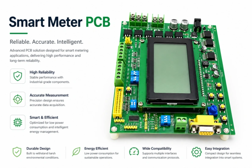
Smart meters communicate through Advanced Metering Infrastructure (AMI) networks. The communication technology varies by region and utility: Sub-GHz RF mesh (Wi-SUN, Zigbee, proprietary at 868/915/920 MHz), power line communication (PRIME, G3-PLC, OFDM-based), NB-IoT, LTE-M, or combinations.
Communication Board Integration
- Sub-GHz RF Mesh: Compact PCB trace antennas or chip antennas at 868/915/920 MHz. Ground plane extension of λ/4 (≈80 mm at 915 MHz) around the antenna element for adequate radiation efficiency. RF matching network (pi or L-network) within 3 mm of the transceiver IC. 50 Ω impedance-controlled feed line. HILPCB fabricates metering boards with antenna sections on controlled-impedance layers while maintaining standard FR-4 construction on metrology layers.
- Power Line Communication: PLC coupling signals (CENELEC A-band 3–95 kHz for EU, or FCC band 10–490 kHz for North America) injected through a coupling transformer onto the mains. The PCB routes high-voltage AC-coupled signals requiring ≥4 mm creepage between PLC line-side traces and low-voltage MCU-side traces. The coupling transformer's primary-secondary isolation must withstand the meter's rated impulse voltage (6 kV typically). PLC analog front end requires careful ground management — the line-referenced ground must be isolated from the meter's safety-rated low-voltage ground.
- NB-IoT / LTE-M Cellular: Cellular modules (Quectel BC660K, u-blox SARA-R5) with USIM card holder and antenna. RF traces at 700–2600 MHz — controlled impedance, ground plane continuity, and via stitching along the RF path. Module placed near the board edge for antenna proximity. Power supply filtering — cellular modules draw 1–2 A peaks during TX bursts that can sag the entire meter's supply rail if not properly decoupled.
- Dual-Stack Coexistence: Meters with RF + PLC (common in European AMI deployments) require careful frequency planning. PLC signals generate broadband noise through the coupling transformer that can desensitize the RF receiver. Supply isolation (separate LDOs for RF and PLC), physical separation (≥15 mm between PLC coupling section and RF antenna), and time-division scheduling prevent interference.
Anti-Tamper Hardware Design
Revenue protection engineering addresses deliberate attacks. Strong magnets placed near CTs saturate the core, reducing measured current by 20–80%. Terminal bypass with external wires diverts load current around the shunt. Neutral disconnection prevents the meter from measuring energy. Board modification or component removal disables measurement or communication. These attacks cost utilities billions annually worldwide.
Tamper Detection PCB Features
- Magnetic Tampering Detection: Hall-effect or GMR sensors on the PCB positioned near each CT — detecting external DC magnetic fields above a threshold (typically >50 mT). Dual sensors per CT (one on each side) distinguish external magnets from transient fields. Sensor conditioning circuits include filtering to reject 50/60 Hz fields from the mains while responding to DC fields within 100 ms.
- Cover and Terminal Tamper: Micro-switches or optical sensors triggering tamper events logged in non-volatile memory with RTC timestamps. The tamper log must be write-protected against firmware modification — hardware-based event capture using dedicated MCU interrupt pins with FIFO buffering ensures events are recorded even if the main firmware is compromised.
- Redundant Current Measurement: Some meter architectures measure current through both a shunt and a CT on the same phase. Disagreement beyond a calibrated threshold triggers a tamper event. The PCB must accommodate both sensors with independent analog front end paths — adding board area and cost, but providing tamper detection that software-only approaches cannot achieve.
- Physical Board Protection: Conformal coating over critical measurement traces prevents probing and modification. Component designators and values not printed on the board's silkscreen. Test points accessible only through sealed compartments in the meter housing. Critical firmware stored in secure elements (ATECC608B or equivalent) with anti-tamper meshes.
High-Voltage Isolation Under IEC 62052/62053
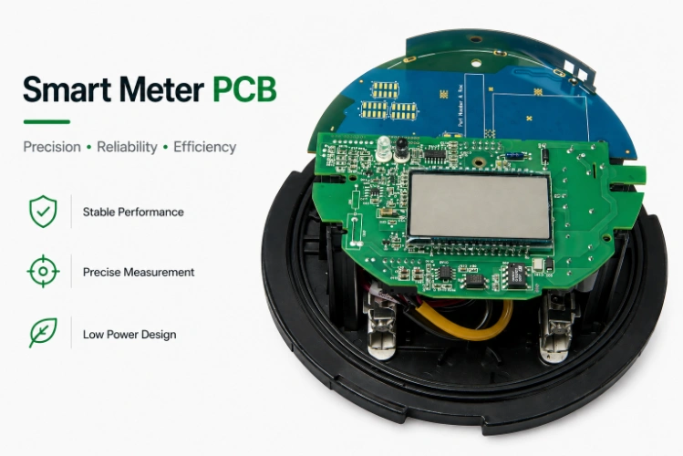
Smart meters connect to mains voltage (120/230/400 V AC, up to 690 V for industrial three-phase). IEC 62052-11, IEC 62053-21/22/23, and UL 2735 define safety isolation, impulse withstand, and environmental requirements.
Safety Implementation on the PCB
- Reinforced Isolation: ≥6 mm creepage and ≥4 mm clearance between mains-referenced metrology circuits and user-accessible communication/display sections under Pollution Degree 2. HILPCB's CNC routing holds slot widths to ±0.1 mm with solder mask pullback preventing fiber tracking along cut edges.
- Impulse Withstand: IEC 62052-11 specifies 6 kV/1.2/50 µs impulse on mains terminals. TVS diodes and MOVs at the board entry point — traces rated for surge current without fusing. Wide copper pours under surge protection components provide low-impedance discharge paths. Via connections from surge components to the ground plane must handle peak currents of 100+ A for microseconds without via failure.
- Hi-Pot Production Testing: Every production board tested at 4 kV AC for 60 seconds between mains and low-voltage sections. This test catches manufacturing defects — solder splash, flux residue bridges, under-etched copper — that reduce effective creepage. 100% testing, no statistical sampling.
- Relay Drive Isolation: Load disconnect relays (for prepaid or demand-response meters) switch mains current. Relay coil drive traces on the low-voltage side must maintain safety spacing from relay contact traces on the mains side. The relay's own package provides internal isolation — but the PCB traces must not compromise it.
20-Year Reliability Engineering
The 20-year field life requirement affects every material and process choice. Components and processes that work fine for 5-year consumer products fail catastrophically when extrapolated to 20 years of continuous operation at elevated temperature and humidity.
Long-Life Design and Manufacturing
- Electrolytic Capacitor Elimination: Aluminum electrolytic capacitors lose capacitance at 5–15% per decade at 85°C due to electrolyte evaporation. After 20 years, a 470 µF electrolytic might measure 300 µF — causing power supply instability or communication failures. Solid polymer capacitors (stable for 20+ years), ceramic capacitors (essentially infinite life), and film capacitors replace aluminum electrolytics wherever possible.
- CAF-Resistant Laminates: Conductive Anodic Filament formation — copper filaments growing along glass fiber/resin interfaces under sustained DC bias in humid conditions — is a leading cause of field failures in meters after 10–15 years of service. The failure mode appears as sudden insulation resistance breakdown between adjacent traces or between different copper layers. CAF-resistant laminate constructions using spread glass weave, high-resin-content prepreg, or alternative fiber treatments eliminate the straight-line glass fiber paths that CAF preferentially follows.
- High-Tg Laminates: Tg ≥ 170°C with Td ≥ 340°C and z-axis CTE ≤ 3.0% (50–260°C). These properties maintain via barrel integrity and copper-to-resin adhesion through 20 years of daily temperature cycling between outdoor ambient extremes. Standard 140°C Tg FR-4 shows measurable via barrel fatigue after 5–7 years of outdoor exposure.
- Solder Joint Long-Term Reliability: SAC305 lead-free solder joints under thermal cycling (worst case: -40°C to +85°C daily outdoor cycles for 20 years = ~7,300 cycles). BGA and QFN packages with underfill adhesive providing mechanical reinforcement against cyclic thermal stress. HILPCB performs accelerated thermal cycling qualification (1,000 cycles at -40°C/+125°C) on representative test vehicles for each meter platform, with microsection analysis at 250-cycle intervals tracking crack propagation.
- Ionic Contamination Control: Flux residues on the assembled board create conductive paths that grow over years of elevated temperature and humidity exposure. HILPCB's assembly process includes post-reflow aqueous cleaning with ionic contamination verification below 1.56 µg NaCl/cm² per IPC-TM-650 — with tighter limits (≤1.0 µg) available for 20-year outdoor applications.
Manufacturing for Utility-Scale Deployment
Production Capability
- Pilot Production: 500–2,000 units supporting type testing and field trials per IEC 62052/62053. DFM review identifying potential long-term reliability risks before volume commitment.
- Volume Production: 10,000–100,000+/year with automated SMT assembly, bed-of-nails ICT, functional metrology verification (accuracy testing at calibration currents), and hi-pot isolation testing integrated into the production line.
- Traceability: Each board serialized with laser marking. Full traceability from laminate lot through assembly — supporting 20-year warranty claims, field failure root cause analysis, and regulatory audit requirements.
- Regional Compliance Documentation: HILPCB supports documentation packages for MID (EU Measuring Instruments Directive), ANSI C12.20 (North America), IS 16444 (India), and regional certification requirements across Southeast Asia, Africa, and Latin America.
Start your smart meter PCB program with a 20-year reliability review →
Frequently Asked Questions
How do smart meter PCBs achieve 20-year field reliability? To survive 20 years outdoors, smart meter PCBs replace failure-prone aluminum electrolytic capacitors with solid polymer or ceramic alternatives. They also use high-Tg, CAF-resistant laminates to prevent via barrel fatigue and conductive anodic filament growth during decades of thermal cycling and humidity exposure.
Why is Kelvin routing important in metrology front ends? In single-phase meters using shunt resistors, a 4-wire Kelvin connection is routed on dedicated layers directly to the metering IC. This separates the low-current sense path from the high-current power path, preventing parasitic trace resistance from introducing millivolt-level offset errors into the measurement.
How are smart meter PCBs protected against physical tampering? PCBs incorporate Hall-effect sensors to detect magnetic tampering, micro-switches for cover removal detection, and redundant current measurement paths. Additionally, critical traces are often protectively coated, and sensitive components lack silkscreen identifiers to thwart reverse engineering.
What isolation standards must smart meter PCBs meet? Smart meters connected to mains voltage must comply with IEC 62052/62053 standards. This requires reinforced isolation with ≥6 mm creepage distances, often achieved through CNC-routed slots. The PCB and its surge protection components must also withstand 6 kV impulse transients from lightning strikes on the power grid.