HILPCB delivers advanced smartphone PCB manufacturing solutions for mobile telecommunications, consumer electronics, and wearable devices. Our expertise encompasses HDI mobile PCB fabrication, flexible circuit integration, and precision assembly that enable compact, high-performance mobile devices. From flagship smartphones to IoT applications, we provide manufacturing excellence for today's demanding mobile electronics market.
Smartphone PCB technology drives mobile innovation, enabling 5G connectivity and AI processing in ultra-compact form factors. These sophisticated boards integrate thousands of components while maintaining exceptional performance and reliability. HILPCB combines cutting-edge manufacturing capabilities with deep mobile electronics expertise to deliver smartphone PCBs that exceed industry standards.
Smartphone PCB Design Requirements
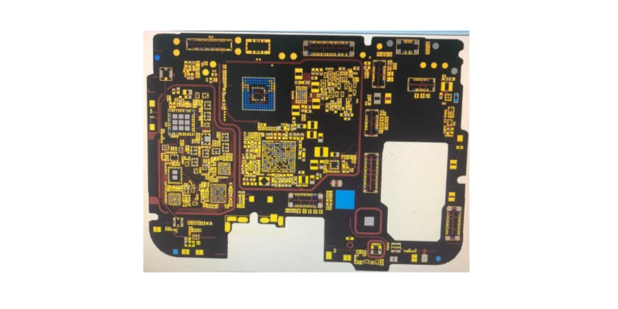
Modern smartphone PCB design demands exceptional miniaturization while supporting complex functionality. Flagship smartphones integrate over 2000 components on boards under 100 square centimeters, requiring precise orchestration of processors, memory controllers, power management, and wireless communication chipsets.
Core Technical Specifications:
• HDI Construction: 8-12 layer designs with microvias down to 75μm for maximum routing density • Ultra-Fine Pitch: BGA packages <0.4mm pitch requiring ±25μm placement accuracy • High-Speed Memory: DDR4/DDR5 interfaces at 3200+ MT/s with ±0.05mm length matching • Multi-Standard Wireless: Integrated 5G, WiFi 6E, Bluetooth, GPS, and UWB support
HDI PCB technology enables via-in-pad designs that maximize routing beneath large processors while maintaining signal integrity. Sequential build-up construction creates complex stackups supporting thousands of connections in minimal space.
Critical Design Factors:
Power delivery networks support processors transitioning from 10mW standby to 5W+ peak loads within microseconds. Thermal management distributes heat across board area while preventing performance throttling. Signal integrity management controls EMI between densely packed wireless subsystems operating across multiple frequency bands.
Manufacturing Processes for High-Density Mobile Devices
Smartphone PCB manufacturing leverages advanced fabrication technologies to achieve ultra-fine geometries and tight tolerances essential for mobile applications.
Advanced Materials:
High-frequency PCB materials maintain stable electrical properties across temperature extremes while preserving signal quality for millimeter-wave 5G interfaces. Flex PCB technology enables foldable displays and wraparound antennas with polyimide circuits surviving hundreds of thousands of flex cycles.
Precision Manufacturing:
• Ultra-Thin Substrates: 0.1mm core materials for compact stackups • Advanced Surface Finishes: ENEPIG for fine-pitch component planarity • Impedance Control: ±5% tolerance for critical high-speed interfaces • Quality Systems: Automated optical inspection and comprehensive electrical testing
Sequential lamination processes create complex via structures optimizing routing density. Laser direct imaging achieves trace widths below 75μm with precise layer registration critical for via-in-pad designs.
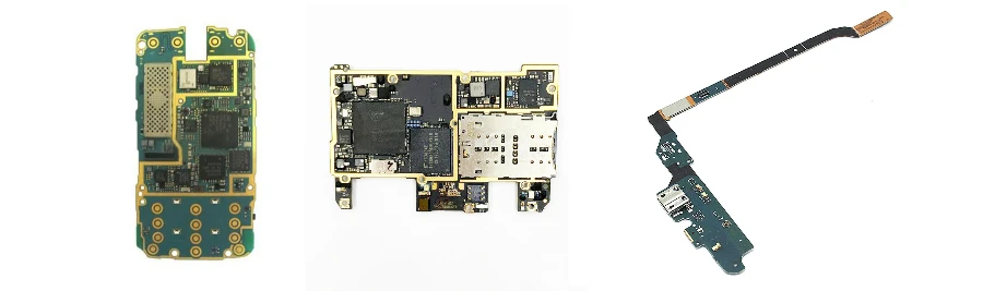
Assembly Solutions for Mobile Device Manufacturing
Smartphone PCB assembly represents pinnacle surface mount technology, handling diverse components from microscopic passives to sophisticated camera modules and wireless chipsets.
Precision Assembly Technologies:
SMT assembly systems employ advanced vision compensation for substrate warpage, ensuring optimal placement accuracy. Multi-zone reflow profiles optimize solder joints across varying thermal masses while protecting temperature-sensitive MEMS sensors and camera modules.
Critical Integration Capabilities:
• Application Processors: Advanced SoCs with thousands of connections • Memory Stacking: Package-on-package (PoP) for maximum density • Camera Systems: Multi-module placement with precision alignment • RF Components: Shielded circuits with controlled impedance transitions
Rigid-flex PCB assemblies enable innovative smartphone architectures supporting folding, sliding, and rotating mechanisms. Comprehensive testing validates functionality across operating conditions with environmental stress screening and drop testing.
Applications in Mobile Communications and Consumer Electronics
Smartphone PCBs enable advanced mobile applications from basic communication to sophisticated computing platforms rivaling desktop performance while maintaining all-day battery operation.
5G Wireless Systems:
Fifth-generation cellular technology demands specialized substrates for millimeter-wave frequencies and antenna integration. Multiple antenna arrays enable MIMO configurations maximizing throughput. Backplane PCB techniques provide high-speed interconnections in modular smartphone designs.
Advanced Integration:
Modern smartphones feature sophisticated camera systems with computational photography, depth sensing, and LiDAR capabilities. AI processing enables real-time image recognition and augmented reality applications. Miniaturized technologies support wearable devices including smartwatches and AR glasses.
Professional Manufacturing Services and Quality Assurance
HILPCB provides end-to-end smartphone PCB solutions from design optimization through high-volume production, supporting global mobile device manufacturers with accelerated time-to-market and guaranteed quality.
Engineering Excellence:
Our technical team delivers signal integrity analysis, thermal simulation, and design-for-manufacturing optimization. Rapid prototyping within 24-72 hours enables quick concept verification. Component obsolescence management and supply chain expertise ensure production continuity.
Manufacturing Capabilities:
Turnkey assembly services manage complete production from component sourcing to final testing. ISO 9001:2015, IPC-A-610 Class 3, and IPC J-STD-001 certifications ensure consistent quality. Flexible systems accommodate prototype to multi-million unit volumes.
Quality Commitment:
Comprehensive testing protocols validate performance across temperature extremes, humidity exposure, and mechanical stress. Environmental compliance includes RoHS, REACH, and conflict mineral reporting. Counterfeit prevention programs protect brand integrity and ensure reliable field performance.
Frequently Asked Questions About Smartphone PCB
Q: What makes smartphone PCB manufacturing unique compared to other electronics?
A: Smartphone PCBs require extreme miniaturization with 15+ components per square centimeter, ultra-fine 0201 components with <0.3mm BGA pitches, and HDI construction supporting thousands of connections. Integration of RF circuits, power management, and high-speed digital interfaces demands specialized expertise and rigorous quality standards.
Q: How do you ensure thermal management in compact smartphone designs?
A: Strategic component placement distributes heat sources while thermal via arrays conduct heat to chassis elements. Advanced materials provide enhanced thermal conductivity. Thermal simulation during design predicts hot spots and optimizes heat spreading within severe space constraints.
Q: What HDI capabilities are essential for modern smartphone PCBs?
A: Critical technologies include microvias <100μm diameter, via-in-pad designs for maximum routing density, and sequential build-up enabling 8-12 layers in thin profiles. Controlled dielectric materials ensure signal integrity while laser imaging achieves ultra-fine geometries for dense component placement.
Q: Can you support both flagship and budget smartphone requirements?
A: Yes, we provide scalable solutions from premium HDI designs for flagship devices with latest processors and 5G to cost-optimized designs for budget smartphones using simplified stackups. Manufacturing capabilities accommodate all market segments while maintaining appropriate quality standards for each application.