

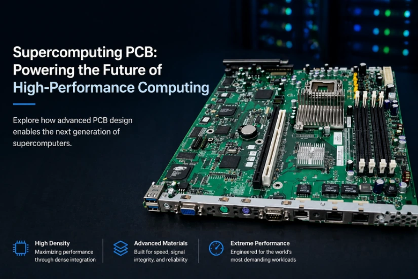
A supercomputing PCB is a high-layer-count circuit board used in compute, accelerator, switching, storage, management or power subsystems whose signal integrity, power delivery, cooling and serviceability are designed as one system. “Exascale” describes aggregate computing performance; it does not define one layer count, laminate, copper weight, flatness limit or qualification plan for every board.
Key Takeaways
- Separate compute/accelerator, switch, backplane, storage, management and power boards before choosing a stackup; their dominant constraints differ.
- 112 Gb/s PAM4 is approximately 56 GBd with a 28 GHz Nyquist frequency. 224G-class PAM4 is approximately 112 GBd with a 56 GHz Nyquist frequency.
- Derive laminate, copper profile, trace geometry, via design and reach from the complete channel budget and SerDes specification—not a universal dB/in or stub limit.
- Model the accelerator power distribution network from rack/bus input through voltage regulators, package and silicon load. Blanket 4–6 oz copper can conflict with fine-line escape and is not the only high-current solution.
- Treat liquid cooling as a mechanical, fluid, reliability and service interface. Cold-plate load, coolant envelope, leak detection and condensation controls belong in the product specification.
- Measure critical-to-quality fabrication parameters with impedance/loss coupons, backdrill structures, registration targets and microsections that represent the released board.
- Use flyover cable, near-package optics or co-packaged optics when long copper reach consumes the channel budget; a more expensive laminate cannot recover every architecture.
- Plan material lifecycle, alternates, firmware/test revisions and spare-build evidence instead of promising an unverifiable decade-long identical process.
Table of Contents
- Define the Supercomputing Board Type
- Build an Interface-to-Evidence Matrix
- Design 112G and 224G PAM4 Channels Correctly
- Choose Laminate, Copper and Glass Weave from the Loss Budget
- Engineer Vias, Backdrilling and HDI Escape
- Know When Copper Routing Is No Longer the Best Link
- Design Accelerator Power Delivery as a Full PDN
- Integrate Liquid Cooling Without Inventing PCB Rules
- Control Board Mechanics Under Cold Plates and Connectors
- Co-Design SI, PI, Thermal and Mechanical Constraints
- Create a Manufacturing Evidence Plan
- Qualify Assembly and System-Level Test Coverage
- Plan Fleet Reliability and Lifecycle Support
- Diagnose Common Supercomputing PCB Failures
- Supercomputing PCB RFQ Checklist
- Reference Standards and Responsibility Boundaries
- How HILPCB Supports Supercomputing PCB Programs
- FAQ
- Conclusion
Define the Supercomputing Board Type
“Supercomputing PCB” covers boards with different optimization targets.
| Board type | Primary functions | Dominant PCB constraints | Evidence that matters |
|---|---|---|---|
| Compute motherboard | CPUs, memory, management, storage and accelerator links | Memory timing, PCIe/CXL reach, socket mechanics, PDN | Timing/channel compliance, PDN impedance, warpage and thermal data |
| Accelerator module/baseboard | GPUs/accelerators, HBM interface, dense power conversion | Fine-pitch escape, fast load transients, cooling load | Package-board co-design, transient response, assembly/warpage evidence |
| Network switch | Switch ASIC, pluggable or co-packaged optics, control plane | SerDes loss, crosstalk, via/connector discontinuities | S-parameters, COM or vendor channel metric, PRBS/BER margin |
| Backplane/midplane | Long multi-connector links and power/control distribution | Reach, connector launches, backdrill, repairability | End-to-end channel model and representative test vehicles |
| Storage/I/O controller | PCIe/CXL/NVMe fanout and connectors | Connector density, retimers, hot-plug, management | Protocol compliance, lane margin and recovery tests |
| Power distribution/conversion | Rack/bus input, intermediate conversion, protection | Current path, creepage, loss, heat and connectors | Milliohm mapping, thermal rise, protection/fault testing |
| Management/security board | BMC, telemetry, root of trust, service interfaces | Availability, secure update, isolation and lifecycle | Recovery, provisioning and configuration traceability |
Do not copy switch-board materials onto a management board or apply blanket heavy copper to fine-pitch escape. Freeze interfaces, reach, power, cooling and service before stackup release.
Build an Interface-to-Evidence Matrix
Connect every critical interface to its reach, manufacturing controls and validation method.
| Interface | Reach/topology inputs | PCB design controls | Manufacturing evidence | System evidence | Change trigger |
|---|---|---|---|---|---|
| 112G PAM4 SerDes | SerDes class, package, PCB length, vias, connectors/cable | Loss/impedance/crosstalk model, smooth copper, via optimization | Impedance/loss coupon, stackup/material lot, backdrill structure | S-parameters plus specified COM/eye/BER test | Laminate, copper, via, connector or equalization |
| 224G-class SerDes | OIF reach class and developing interface requirements | Shorter reach, stricter discontinuity and loss allocation | Higher-bandwidth coupon/fixture de-embedding | End-to-end interoperability and margin | Package/optics architecture or standard revision |
| PCIe/CXL | Generation, lane width, connectors, retimers | Vendor/PCI-SIG channel limits, reference continuity | Coupon and connector/via construction control | Protocol compliance, equalization and error recovery | CPU/retimer/connector or generation |
| Memory | Data rate, topology, package/connector | Timing, crosstalk, power/reference control | Stackup, registration and impedance evidence | Training margin and stress tests | Memory/package/layout or firmware training |
| Core PDN | Load-line, transient spectrum, regulator/package model | Target impedance, low-inductance paths, decoupling | Copper thickness, via/fill and assembly evidence | Rail droop/noise under representative workloads | Silicon, VRM, capacitor or package |
| Cooling interface | Device power map, coolant envelope, mounting load | Keepouts, stiffness, sensor/leak-detection interfaces | Dimensional/warpage evidence as specified | Thermal, pressure/leak and service qualification | Cold plate, TIM, manifold, coolant or board outline |
This prevents a “112G capable” certificate from being mistaken for channel compliance and identifies evidence reopened after a change.
Design 112G and 224G PAM4 Channels Correctly
PAM4 carries two bits per symbol. A 112 Gb/s lane is near 56 GBd/28 GHz Nyquist; a 224 Gb/s-class lane is near 112 GBd/56 GHz. Simulation and measurement must still extend as required beyond Nyquist.
OIF CEI-112G defines multiple reach classes rather than one universal channel. OIF’s CEI-224G work similarly distinguishes extra-short, very-short, medium and long reach architectures. IEEE 802.3ck standardized 100 Gb/s-per-lane electrical interfaces used to build 100/200/400 GbE links. The applicable host/optical-module or chip-to-chip specification determines the loss, return-loss, crosstalk and equalization assumptions.
A channel includes packages, traces, vias, connectors, cables and module interfaces. Allocate loss before layout, then validate causal/passive S-parameters with correct reference impedance and de-embedding. Use a fixed PCB dB limit only when the released budget assigns it.
PAM4 has three eyes and less vertical margin than NRZ at the same signal swing. But bit-error performance depends on transmitter linearity, noise, jitter, crosstalk, reflections, equalization and forward-error correction—not simply insertion loss at one frequency.
Choose Laminate, Copper and Glass Weave from the Loss Budget
Low-loss laminate is often necessary for longer 112G/224G copper channels, but “Df below 0.0015” is not a universal procurement rule. Datasheet Dk/Df values depend on frequency and test method and may not match the design value used by a field solver.
Release exact resin, glass, copper profile, dielectric thickness and alternates. Use construction-specific design Dk/loss inputs. Hybrid stackups can reserve low-loss material for critical layers, but compatibility and processing need qualification.
Copper roughness increases loss. Specify a foil/profile compatible with the model rather than comparing unlike Rz methods; agree on the exact foil and treatment.
Fiber weave can create intra-pair skew and local impedance variation. Mitigations include spread-glass styles, artwork rotation/skew, trace placement and wider geometries. “Route every pair at 10 degrees” is not a universal rule; panel utilization, routing density, weave pitch and measured skew determine the strategy.
Engineer Vias, Backdrilling and HDI Escape
Via stubs create resonances and discontinuities, but the maximum allowable residual stub comes from the channel model. A fixed 5 or 6 mil limit is neither necessary nor sufficient across every layer transition, drill size, antipad, dielectric and interface.
Optimize:
- signal/ground via geometry and return-via placement;
- antipad shape through all reference planes;
- breakout trace and pad transitions;
- finished hole, capture pad and registration allowance;
- backdrill side, target layer, depth tolerance and copper clearance;
- connector launches and press-fit compliant-pin fields;
- unused pads and plane cavities where removal is qualified.
Use 3D EM models for critical launches. Define backdrill intent, residual stub, overshoot protection, inspection method and sampling in the fabrication drawing.
HDI may be required for fine-pitch escape, but stacked microvias add risk. Select structures, pads, fill and cycles from the package breakout and qualified fabrication process.
Know When Copper Routing Is No Longer the Best Link
When package, connector and trace loss consume the budget, the correct answer may be architectural:
| Option | Benefit | Trade-off |
|---|---|---|
| Retimer | Extends reach and restores protocol margin | Power, latency, firmware and validation complexity |
| Flyover cable | Removes a long lossy PCB segment | Connector, assembly, airflow and service constraints |
| Near-package optics | Shortens electrical reach to the optical engine | Thermal, power, fiber routing and serviceability |
| Co-packaged optics | Minimizes switch-ASIC electrical reach | Packaging, optical service, yield and ecosystem complexity |
| Higher-performance laminate | Preserves conventional board architecture | Cost and supply risk; cannot fix poor launches or excessive reach |
OIF’s 112G and 224G projects explicitly separate reach classes because one electrical architecture cannot optimize every path. Run the channel budget before committing board size and connector placement.
Design Accelerator Power Delivery as a Full PDN
Accelerators can draw hundreds of amperes on sub-volt rails, but the PCB should not be reduced to a “4–6 oz copper” prescription. The power path may include rack busbars, 48 V or another distribution voltage, intermediate bus converters, multiphase regulators, vertical power delivery, package substrates and on-package decoupling.
Start with the silicon load-line/transient model. Build a frequency-dependent target-impedance plan through board/package resonances and validate it with impedance, rail captures and representative load steps.
Regional thick copper, coins, busbars, embedded conductors or power modules can preserve fine-line routing elsewhere. Simulate DC resistance, constriction, connector loss, current sharing and heat; one plane-resistance estimate is not a board design.
Decoupling selection must include mounting inductance, capacitor bias/temperature aging, anti-resonance and package interaction. “Place more capacitors” can worsen impedance peaks or consume routing/airflow without improving transient margin.
Integrate Liquid Cooling Without Inventing PCB Rules
Direct liquid cooling moves heat through cold plates and a facility/rack fluid loop. OCP cold-plate guidance emphasizes defined thermal, hydraulic, mechanical, material and reliability interfaces; it does not prescribe one PCB flatness percentage for every system.
Create an interface control document:
| Boundary | Required inputs | Qualification evidence | Primary owner |
|---|---|---|---|
| Device to TIM/cold plate | Power map, die/package limits, contact area, clamp load | Thermal resistance, pressure map and cycling | Silicon/mechanical/thermal |
| Cold plate to board | Mounting datums, load path, keepouts, deflection limit | Board strain/warpage and fastener validation | Mechanical/PCB |
| Cold plate to manifold | Coolant, pressure, flow, QD, hose and service envelope | Pressure drop, leak, burst and cycle tests | Cooling-system team |
| Cooling to facility environment | Supply temperature, dew point, water quality, controls | Condensation risk and facility qualification | Data-center/facility |
| Leak response | Sensors, containment, shutdown and diagnostics | Fault injection and service procedure | System/reliability |
Avoid operating cold surfaces below local dew point unless the system is explicitly designed for condensation control. Conformal coating is not a substitute for coolant containment, leak detection or environmental control. Coating can also trap contamination, obstruct connectors and complicate rework.
Quick disconnects and manifolds require keepouts, hose radius, insertion force and drip management in the 3D baseline before placement.
Control Board Mechanics Under Cold Plates and Connectors
Large packages, sockets, DIMMs, press-fit connectors and cold plates apply loads that can warp the board and strain solder joints. Specify flatness/warpage only from assembly, connector and TIM needs; tighter is not automatically safer or economically achievable.
Use FEA and strain measurements for assembly, cold-plate torque, shipping and service. Define stiffeners, screw sequence/torque, spans and keepouts; transfer load through a designed structure.
Panelization and copper balance influence fabrication warpage; component distribution and reflow influence assembled warpage. A bare-board optical measurement cannot guarantee TIM contact after BGA assembly, socket loading and cold-plate installation. Correlate measurements across the actual sequence.
Co-Design SI, PI, Thermal and Mechanical Constraints
The main HPC layout conflicts occur at shared real estate:
- high-speed SerDes wants short routes, smooth copper and uninterrupted references;
- core PDN wants wide, low-inductance power paths and dense decoupling;
- thermal design wants cold-plate mounts, airflow/coolant access and sensor placement;
- mechanics wants stiffeners, fasteners, connector support and service clearance;
- manufacturing needs copper balance, drill access, coupons, panel rails and testability.
Run joint design reviews before placement freeze. A thermal via field may puncture SerDes reference planes; an oversized power pour may block escape; a backplate may collide with bottom-side decoupling; a manifold keepout may lengthen optical-module traces beyond the budget.
Tie one constraint database to board revision and analysis. Include SI, PI, thermal, mechanical, fabrication, assembly and system sign-off.
Create a Manufacturing Evidence Plan
Instead of advertising a universal Cpk, define critical-to-quality characteristics and the evidence needed for this board.
| CTQ | Production control | Evidence |
|---|---|---|
| Differential impedance | Released stackup, artwork compensation and process control | TDR coupon with limits/correlation |
| Insertion loss | Material/foil/glass control and representative line | Loss coupon or S-parameter test with de-embedding |
| Backdrill residual stub | Registered depth program and drill controls | Coupon, microsection or other agreed inspection |
| Layer registration | Scaling and lamination controls | Targets, X-ray data and microsections |
| Microvia structure | Qualified laser drill/fill/sequential process | Microsections and specified reliability evidence |
| Finished thickness/warpage | Material/copper balance and press cycle | Dimensional report at specified condition |
| Copper/current structures | Foil/plating/fill and geometry control | Microsection, resistance and dimensional evidence |
| Material identity | Approved manufacturer/grade/foil/glass list | Lot traceability and change notification |
Coupons must represent production. An outer-layer 50 Ω line cannot prove a long inner-layer PAM4 channel with vias/connectors. Agree location, orientation, planes and correlation during stackup planning.
Qualify Assembly and System-Level Test Coverage
Large BGAs, bottom-terminated power packages, press-fit connectors and heavy thermal hardware require process-specific inspection.
- Use SPI/AOI and X-ray/AXI with released defect criteria; a generic void percentage is not valid for every ball or thermal pad.
- Correlate reflow profile to the actual board, component mass and laminate limits.
- Provide boundary scan, JTAG, rail isolation and test points before routing closes access.
- Use PRBS, built-in eye/BER diagnostics and protocol tests at system level for high-speed links.
- Capture rail noise, current and thermal sensors during representative compute/network loads.
- Validate cold plate, TIM, pump/flow controls, leak response and service procedures in the assembled system.
Bare-board tests prove fabrication attributes; assembly inspection proves selected workmanship attributes; system tests prove interface margin. None can substitute for the others.
Plan Fleet Reliability and Lifecycle Support
Fleet availability depends on hardware failure rate, telemetry, fault containment, redundancy, repair time and spare strategy. A board MTBF improvement does not translate one-for-one into compute throughput without a system model.
Define mission profiles for temperature, power cycling, coolant, vibration, humidity and service operations. Use appropriate component and interconnect qualification, accelerated tests and field telemetry to update reliability assumptions. Track correctable link errors, rail excursions, thermal throttling, pump/flow alarms and connector replacements before they become outages.
Lifecycle planning should record approved materials and alternates, component PCNs/EOLs, tooling/data retention, firmware/test compatibility and the evidence required for a spare build. No supplier can guarantee an unchanged material/process for a decade without controlled substitutions and requalification rules.
Diagnose Common Supercomputing PCB Failures
| Failure | Common contributors | Evidence to collect | Preventive control |
|---|---|---|---|
| PAM4 link passes short test, fails full path | Wrong reach/loss allocation, via or connector discontinuity | End-to-end S-parameters, COM/BER and segment correlation | Interface-to-evidence matrix |
| Lot-to-lot SI drift | Material/foil/glass or dielectric variation | Coupon trend and lot construction data | Exact approved construction and change control |
| Rail droop under accelerator burst | PDN resonance, VRM/package inductance, capacitor bias | Impedance and time-domain rail/current capture | Full board-package PDN model |
| Cold plate performs inconsistently | Load, TIM, warpage or flow distribution | Pressure/flatness/thermal/flow correlation | Mechanical-fluid interface control |
| Condensation or corrosion | Surface below dew point, leak, contamination | Environmental, coolant and residue evidence | Non-condensing controls, containment and cleanliness |
| BGA/microvia failures after cycling | Warpage, strain or unqualified HDI structure | X-ray, microsection and strain/thermal history | Representative assembly/reliability qualification |
| Backdrill passes drawing but link margin is low | Antipad/launch dominates or coupon is unrepresentative | 3D model and de-embedded measurements | Channel-based via design and representative coupon |
| Spare board is incompatible | Silent material, firmware, optics or test change | Baseline and change-history audit | Lifecycle configuration control |
Supercomputing PCB RFQ Checklist
System and board scope
- Board type, form factor, block diagram, system topology and mechanical model.
- Interface standards/generations, reach classes, channel budgets and connector/cable/optics selections.
- Power states, rail/load-line data, cooling architecture and lifecycle targets.
PCB fabrication
- Gerber/ODB++/IPC-2581, drill/netlist, fabrication drawing and controlled constraints.
- Released regional stackup with exact laminates, glass, foil/profile, copper and approved alternates.
- Impedance/loss tables, via/backdrill structures, HDI cycles, registration and warpage limits.
- Coupon designs, test methods, fixtures/de-embedding, sampling and raw-data requirements.
Assembly and mechanics
- BOM/AVL, package drawings, placement, assembly drawings and 3D data.
- Socket/press-fit/cold-plate/stiffener loads, keepouts, torque and assembly sequence.
- Paste/alloy, reflow, X-ray/AXI, cleaning/coating and rework constraints.
Test and traceability
- Boundary scan, programming, power sequencing, PRBS/BER/protocol and functional coverage.
- Golden units/models, limits, fixture versions, correlation and failure-analysis plan.
- Lot/panel/unit traceability, material identity, deviations and requalification triggers.
Commercial and lifecycle
- Prototype, validation, pilot, production and spare quantities/forecast.
- Long-lead/EOL risks, consigned parts and alternate qualification.
- Separate cost/lead-time effects for low-loss materials, HDI cycles, backdrill, coupons and reports.
- Data/tool retention, PCN/ECO process and future build responsibilities.
Reference Standards and Responsibility Boundaries
Use the specifications applicable to the released interfaces and contract:
- OIF CEI-112G and CEI-224G Implementation Agreements/Projects
- IEEE 802.3ck — 100 Gb/s-per-lane Electrical Interfaces
- PCI Express Base Specification 6.0/7.0 as applicable
- Compute Express Link Specifications as applicable
- OCP ACS Liquid Cooling Cold Plate Requirements and platform guidance
- IPC-2221 / IPC-2222 — Generic and Rigid PCB Design
- IPC-6012 — Qualification and Performance for Rigid PCBs
- IPC-4101 — Base Materials for Rigid and Multilayer PCBs
- IPC-9701 — Surface-Mount Attachment Performance Testing
- IPC-A-610 / J-STD-001 — Assembly Acceptability and Soldering
Interface owners and system architects own channel, PDN, cooling, reliability and lifecycle requirements. The PCB fabricator owns conformance to the released stackup/drawing and disclosed deviations. The assembler owns controlled process execution and inspection. System integrators own protocol margin, coolant safety, thermal performance and fleet availability.
HILPCB can support agreed DFM, stackup collaboration, PCB fabrication, assembly and manufacturing records. HILPCB cannot guarantee exascale performance, a fixed PAM4 reach, fleet uptime, a national-program qualification or decade-long identical materials without project-specific evidence and contractual controls.
How HILPCB Supports Supercomputing PCB Programs
Send HILPCB the board type, interface matrix, released channel/PDN constraints, regional stackup, cold-plate mechanics, CTQ list, coupon plan and test allocation. A useful fabrication review should disclose build limits, material/foil alternatives, HDI/backdrill risks, panel/coupon strategy and measurable acceptance evidence.
Relevant services include high-speed PCB manufacturing, multilayer PCB fabrication, HDI PCB manufacturing, heavy copper PCB fabrication and SMT assembly. Use prototype assembly to correlate models, coupons, assembly and system tests before production. Submit the released package through the PCB quote request.
FAQ
Is the Nyquist frequency of 112G PAM4 56 GHz?
No. PAM4 carries two bits per symbol, so nominal 112 Gb/s PAM4 is about 56 GBd and has a Nyquist frequency near 28 GHz. A 224 Gb/s-class PAM4 lane is about 112 GBd with a Nyquist frequency near 56 GHz. Channel models still need adequate bandwidth beyond Nyquist.
What is the maximum backdrill stub for a 112G PCB?
There is no universal value. The allowed stub depends on the via/antipad geometry, layer transition, material, connector/package channel and the interface’s loss/return-loss requirements. Determine it through the channel model and verify the released fabrication process with representative structures.
Do supercomputing accelerator boards always need 4–6 oz copper?
No. High current may be carried through regional thick copper, multiple planes, busbars, copper coins, embedded conductors, power modules or vertical delivery. Blanket heavy copper can hinder fine-line etching and high-speed stackups. Select the structure from DC resistance, transient inductance, thermal and manufacturing evidence.
What should be included in a liquid-cooled PCB specification?
Define the cold-plate/TIM interface, power map, coolant and supply-temperature envelope, pressure/flow, quick disconnects, keepouts, mounting load, board strain/warpage limits, leak detection, condensation controls, service sequence and qualification responsibilities. A coating or flatness callout alone is insufficient.
Conclusion
Supercomputing PCBs succeed through allocation and evidence, not extreme numbers copied from another platform. Identify the board type, assign each interface a reach and budget, model the entire channel or PDN, and select materials, vias and copper structures that close those requirements.
Then connect the electrical design to cold-plate mechanics, coolant controls, assembly, representative coupons, system margin tests and lifecycle change rules. When copper reach stops closing, change the architecture rather than hiding the gap behind a premium laminate. That evidence chain is what turns a dense high-speed board into a supportable supercomputing subsystem.