
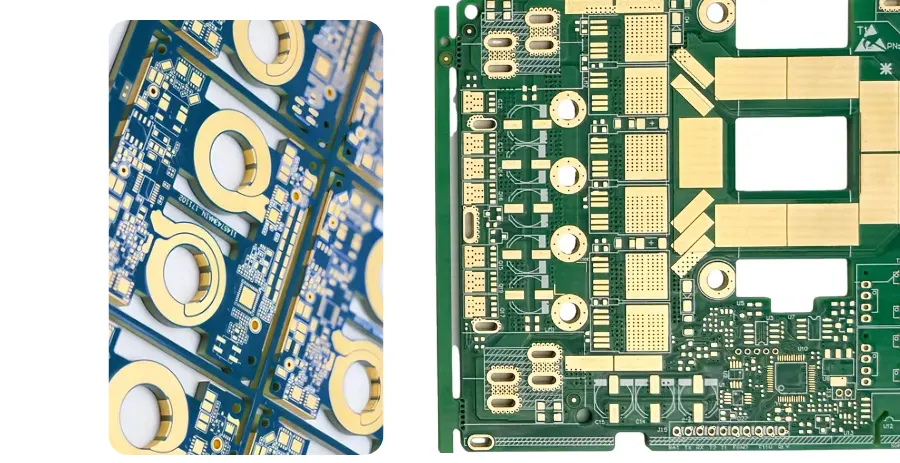
Choose a thick copper PCB when the available routing area cannot meet voltage-drop and temperature-rise limits with a thinner copper construction. Increasing copper cross-section reduces resistance, but a connector, via array or narrow pad entry can still limit the complete power path. Compare a wider trace, parallel layers and an external busbar before committing to heavier copper.
A thick-copper PCB commonly uses finished copper weights of roughly 3 oz/ft² (about 105 µm nominal) or greater; definitions vary by supplier. These boards are engineered for reliability under high current, high temperature, or mechanically stressful environments. They are commonly used in:
- Power supply modules
- EV battery protection and charging systems
- Solar inverter circuits
- Industrial motor controllers
- Military or aerospace-grade systems
Multilayer heavy-copper stacks (for example, 4 oz power layers alongside thinner signal layers) require supplier confirmation of etch capability, via plating, and any customer-specific thermal/vibration qualification. These use cases emphasize the importance of both electrical performance and mechanical reliability under real-world conditions.
1. What Is a Thick Copper PCB and Why Use It?
Heavy copper commonly starts around 3 oz/ft²; there is no single current threshold that defines it. HILPCB’s heavy copper PCB service lists 3–6 oz as its standard copper range and builds up to 20 oz (about 700 µm nominal) for advanced review; HILPCB also has manufacturing experience with 6 oz and hybrid multilayer boards. Specify starting foil and required finished copper separately, layer by layer. These are reviewed routes, not a promise that maximum copper, finest spacing and smallest holes combine.
Use Cases
Heavy copper can be useful in power paths such as:
- DC/DC converters
- Battery management systems
- Industrial drivers and servo controllers
- Power distribution backplanes
- High-voltage energy systems
Why Engineers Choose Thick Copper
- Current handling: Larger cross-section lowers resistive losses
- Heat spreading: More copper can spread heat toward a cooled area; the enclosure still needs a heat-removal path
- Conductor robustness: Thicker tracks can tolerate handling better, while laminate adhesion and plated holes still need appropriate controls
- Transient energy handling: Evaluate pulse duration, repetition and protection clearing time; copper weight alone does not establish a short-circuit rating
- Reduced voltage drop: Better voltage stability in high-load zones
2. Design Guidelines for Thick Copper PCBs
Designing a thick copper PCB isn’t just about increasing copper weight. It impacts layout rules, impedance, stackup construction, and DFM.
a. Trace Width Calculation
Use IPC-2152, Standard for Determining Current Carrying Capacity in Printed Board Design, to assess conductor size against current and acceptable temperature rise. Include layer position, nearby copper, ambient temperature and cooling. For a 10 A path on 4 oz copper, there is no universal width without those conditions. Check the minimum finished cross-section after etching, then validate the assembled board in its enclosure.
A separate voltage-drop check helps expose bottlenecks: Vdrop = I × R and Ploss = I² × R. As an illustrative assumption, a complete 10 mΩ power path carrying 20 A drops 0.20 V and dissipates 4 W. If conductor resistance alone is halved, its voltage drop and heating halve at the same current; unchanged connector and via resistance does not. Use resistance at operating temperature and include both supply and return paths. This calculation is an electrical budget, not an ampacity or thermal qualification.
b. Heat Management
Thick copper helps conduct heat, but copper spreading, suitable via arrays and a path to the heatsink or ambient still determine steady-state temperature. Check neck-downs at terminals and component pads. Distributing current between layers may help, provided the connecting vias can carry the transfer current and share it as intended.
c. Minimum Spacing and Etchability
Thicker copper generally needs more etch allowance and resin clearance. A single trace/space rule cannot be assigned from copper weight alone: the result depends on starting foil, plating buildup, layer position and the etch process. Ask CAM to confirm the smallest finished conductor width and spacing on each power layer, including local constrictions.
Do not transfer a fine-line value from a general capability chart to a 20 oz layer. Also check electrical clearance and creepage from the voltage, environment and product requirements; an etchable gap is not automatically a safe insulation distance.
d. Balanced Stackup Design
Balance copper weight and copper coverage about the stackup center where practical. Matching nominal weights alone does not balance a nearly solid plane against a sparse routing layer. For mixed signal/power stacks, review resin fill between thick features, dielectric thickness after lamination and bow/twist limits. A 6 oz outer layer does not impose one fixed inner-layer weight; approve the actual stackup with the fabricator.
3. Key Considerations When Sourcing Thick Copper PCBs
a. DFM and Stackup Validation
At HilPCB PCB Factory, we help customers validate stackups before production. We consider:
- Resin flow under high copper weight
- Layer bonding temperature and Tg rating
- Hole wall plating for thick-layered designs
Early engagement avoids surprises during manufacturing.
b. Quality and Reliability Standards
Specify the applicable IPC-6012 revision, performance class and any additional drawing requirements. HILPCB offers 100% electrical testing, AOI, impedance testing and cross-section inspection; optional thermal-cycle reports can be quoted when specified. Agree test structures, deliverables and sampling plan rather than assuming every report is included.
- Copper thickness: the service page lists ±10% plating uniformity as a process reference. Define the required minimum finished copper, measurement locations and acceptance tolerance for this stackup; do not treat that reference as a universal tolerance on every conductor or hole barrel.
- Plated holes: state finished-hole dimensions and minimum barrel copper separately from planar copper weight. Cross-sections can examine the agreed structures.
- Electrical performance: specify continuity/isolation testing, and impedance coupons where controlled-impedance signal layers are part of the build.
- Reliability evidence: identify any thermal cycling, load testing or microsection reports needed for release, including the test conditions and who approves the results.
c. Lead Time and Capacity
The heavy-copper service lists a 7–10 working-day prototype reference. Other reference schedules are 10–14 working days for low-volume production and up to 18 working days for mid-volume production. HILPCB confirms the order schedule after stack-up, material, CAM and capacity review; request eligible rush review where needed. Distinguish fabrication from sourcing, assembly, qualification testing and transit.
d. Cost Drivers and Quoting Advice
Factors affecting cost:
- Copper foil, plating buildup and any additional lamination cycles
- Hole aspect ratio, drill wear and plating requirements
- AOI and etch tolerance adjustments
To optimize cost:
- Use only the copper weight you need
- Combine signal and power with hybrid stackups
- Ask for standard material options if possible
We offer transparent quotations with stackup details, and engineering suggestions to reduce cost without sacrificing reliability.
e. Shipping and Handling
HILPCB can provide vacuum or ESD packaging, rigid-board protection, customs pack-out and global shipment; combined PCB and PCBA shipments can be arranged with item-level traceability. Include board mass, quantity and destination in the RFQ, and agree moisture protection, separation and edge protection. Compare freight and tooling with the board price.
4. Thick Copper PCB Assembly: Real-World Adjustments for Reliable Production
a. Reflow and Thermal Mass
Heavy copper increases thermal mass, so a profile suitable for a thin signal board may leave power joints insufficiently heated. Conversely, simply extending the soak or raising the oven setting can exceed a nearby component’s exposure limit.
HILPCB can tune the assembly profile in-house using a representative populated assembly, including a large copper-connected joint and temperature-sensitive components. Keep ramp, soak, time above liquidus and peak within paste and component specifications. For selective soldering, check preheat, flux access and nozzle clearance. Stencil changes should follow paste-transfer and joint-volume needs rather than copper weight alone.
b. Pad Design and CAM Optimization
Thermal relief can improve solderability, but each spoke also constricts the current path. Calculate its resistance and heating before replacing a solid plane connection. Select solder-mask-defined or non-solder-mask-defined lands from the component and fabrication requirements; neither is a general heat-control solution.
Open vias in solderable pads can wick solder away. Where via-in-pad is needed, specify an appropriate filled and capped construction and its inspection criteria. HILPCB provides CAM layout advice and coordinates pad geometry, hole position, mask and assembly sequence through DFM review before changing the released layout.
Conclusion: Manufacturability Starts With Engineering Awareness
For a motor controller, battery module or solar converter, send the fabrication data, netlist, layer stackup, copper requirements and quantity through the heavy copper PCB service. Include continuous and peak currents with pulse duration, allowable voltage drop, ambient/cooling conditions, operating voltage and any assembly or load-test scope.
Ask the quotation to return a proposed finished stackup, confirmed power-layer trace/space, hole and plating limits, inspection deliverables, open DFM items and a release-based schedule. That gives purchasing a comparable manufacturing scope and gives engineering a clear list of decisions to close before production.
Frequently Asked Questions
Does a high-current PCB always need heavy copper?
No. Current capacity depends on finished conductor cross-section, cooling and the allowed temperature rise. Wider traces, parallel copper layers or a busbar may meet the requirement. Heavy copper is useful when the board area or loss budget makes thinner copper impractical. Check connectors, vias, protection devices and the return path as well as the main trace.
Can 20 oz copper use the same design rules as 3 oz copper?
Do not assume so. Ask the fabricator to approve finished trace width, spacing, holes, resin fill and stackup for each copper weight. HilPCB lists builds up to 20 oz, but the complete combination must pass engineering review.