
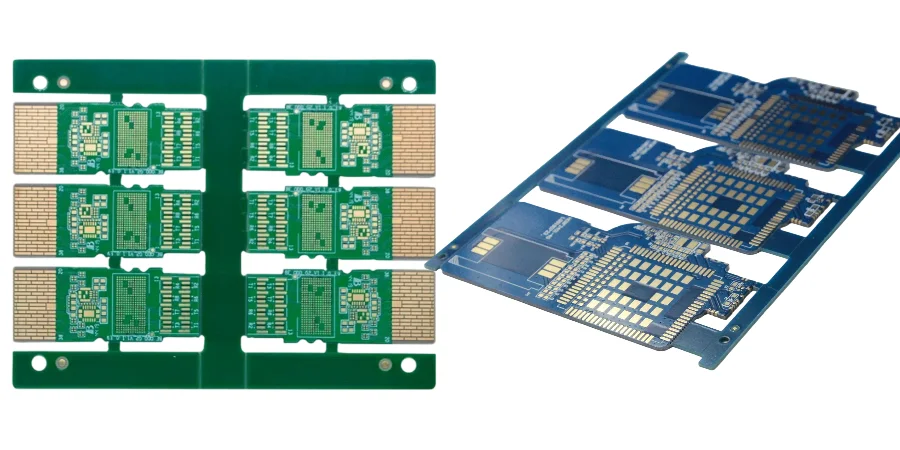
A high-speed TIA/LA receiver board is one of the most sensitive hardware areas inside a modern optical module. It sits at the boundary between weak photodiode current, low-noise analog amplification, high-speed electrical output, digital management, thermal constraints, and host-interface expectations. A receiver board that looks acceptable as a schematic can still fail in production if the PCB layout, thermal path, power noise, CMIS data, inspection flow, and module-level validation are not planned as one system.
This guide explains how to review a high-speed TIA/LA receiver board for data center optical modules without overstating what the PCB alone can prove. The board can support receiver sensitivity, signal integrity, thermal stability, EEPROM/CMIS management, and repeatable PCBA manufacturing. It does not, by itself, prove full optical-module interoperability, host compatibility, Ethernet compliance, or MSA conformance. Those outcomes require module-level electrical, optical, firmware, thermal, and host testing.
Key takeaways
- A TIA/LA receiver board is a mixed-signal, optoelectronic PCB problem: photodiode input noise, TIA gain stability, LA output quality, DSP handoff, firmware control, and thermal path all interact.
- QSFP-DD, OSFP, and similar form factors set mechanical, electrical, pinout, and thermal constraints, but a PCB layout is only one part of meeting those module-level requirements.
- CMIS compatibility depends on accurate management-interface implementation, memory map behavior, firmware configuration, telemetry scaling, alarms, and host interpretation—not just EEPROM programming.
- Thermal design must protect receiver sensitivity. Heat from the DSP, laser driver, TEC driver, or module cage can shift receiver noise and gain behavior if the TIA/LA area is not isolated and conducted properly.
- Manufacturing must be planned around small components, fine-pitch packages, controlled impedance, X-ray coverage, programming, calibration, functional testing, and traceability.
In this guide
- What a TIA/LA receiver board actually does
- Form factor and MSA constraints
- Receiver signal-chain layout
- Thermal path and temperature sensitivity
- Power integrity and noise control
- CMIS, firmware, EEPROM, and telemetry
- Manufacturing, inspection, and validation flow
- Common failure modes
- Cost drivers and RFQ checklist
- FAQ
What a TIA/LA receiver board actually does
A receiver-side optical module board converts a very small optical signal into a usable high-speed electrical signal. The front end usually begins with a photodiode or photodiode array. The current from that device enters a transimpedance amplifier, or TIA, which converts weak current into voltage while preserving signal bandwidth and minimizing added noise. A limiting amplifier, or LA, may then condition the signal to the expected output level or prepare it for a DSP, CDR, retimer, or host-side electrical interface.
That chain is easy to describe but hard to implement. The photodiode input node is often one of the most noise-sensitive nodes in the module. It can be disturbed by power ripple, ground bounce, clock harmonics, laser-driver switching, DSP heat, EMI from nearby high-speed lanes, contamination, and mechanical stress around the optical sub-assembly. Once noise is coupled into the first stage, later equalization cannot fully recover the lost receiver margin.
A practical receiver-board review should therefore start with signal-chain ownership:
| Receiver area | Main PCB concern | Manufacturing concern | Validation evidence |
|---|---|---|---|
| Photodiode input | Ultra-short, shielded, low-capacitance path into the TIA | Clean assembly, no flux residue near high-impedance nodes | Receiver sensitivity, optical modulation amplitude, BER or error-rate margin |
| TIA supply and bias | Low-noise supply, local filtering, stable reference | Correct capacitor values and placement, solder integrity | Supply-noise measurement, gain stability, temperature sweep |
| TIA output / LA input | Controlled impedance, clean return path, low crosstalk | Fine-pitch placement, BGA/QFN inspection where used | Eye, jitter, S-parameter or link margin tests |
| LA output / DSP handoff | Matched differential routing and via discipline | AOI/X-ray/ICT/FCT coverage | Host-side electrical margin and module functional tests |
| MCU and management | Telemetry, alarm logic, EEPROM/CMIS behavior | Programming and data verification | CMIS read/write checks and host recognition tests |
This is why the phrase TIA/LA receiver board design should not be treated as only a high-speed routing problem. It is a board-level integration problem that includes low-noise analog layout, controlled impedance, power sequencing, thermal conduction, firmware interaction, and production data control.
Form factor and MSA constraints
Pluggable optical modules must fit into tightly defined mechanical and thermal envelopes. For example, QSFP-DD and OSFP are form-factor ecosystems that define aspects such as mechanical module geometry, cage interface, electrical connector behavior, pinout, and thermal expectations. The PCB designer cannot treat the receiver board as a free-form high-speed board; it has to survive inside a metal shell with limited airflow, fixed host connector locations, strict keepout areas, and a short thermal path to the cage or heat sink.
The most important point is scope. A PCB supplier can help manufacture a board that supports a QSFP-DD, OSFP, or other module design. The PCB alone does not prove the module meets the MSA. That proof requires the full module assembly, cage/host interaction, firmware, power, thermal, electrical, and optical testing.
MSA-driven PCB constraints
| Constraint | Why it matters to receiver-board layout | Practical PCB response |
|---|---|---|
| Fixed module length and width | Limits room for TIA/LA, DSP, MCU, memory, power, and test pads | Use HDI, stacked/buried vias, dense component placement, and rigid-flex only when justified |
| Cage and housing thermal path | Determines where heat can leave the module | Put heat-generating devices under usable thermal contact areas; avoid trapping receiver heat |
| Host connector location | Forces short, high-speed transition planning | Keep host-side differential pairs disciplined and avoid unnecessary layer changes |
| Optical engine location | Controls ROSA/TIA placement and fiber alignment stress | Minimize photodiode-to-TIA length and avoid stress transfer into sensitive receiver nodes |
| Management interface pins | Requires clean low-speed digital routing and pull-up strategy | Plan I2C/MDIO, reset, interrupt, low-power mode, and module-select routing early |
| Test access | Space is limited, but production needs evidence | Reserve compact programming, calibration, and functional test access before layout freeze |
For compact optical modules, HDI PCB and rigid-flex PCB are often used to reduce routing congestion, remove board-to-board connector penalties, or connect optical sub-assemblies to the main board. They should be selected based on actual package escape, bending reliability, stackup control, and assembly yield—not just because the module sounds advanced.
Receiver signal-chain layout
The receiver chain is vulnerable because the most sensitive signal is encountered before the board has a chance to clean it up. A good layout protects the photodiode input and TIA environment first, then controls the high-speed outputs and digital management interfaces.
Photodiode-to-TIA region
The photodiode input path should be short, shielded, and isolated from switching nodes. Keep parasitic capacitance low because capacitance at the TIA input can reduce bandwidth and increase noise sensitivity. Avoid routing aggressive clocks, DC-DC switching nodes, laser-driver currents, or host-side high-speed lanes under or next to the photodiode input area unless the stackup and shielding strategy are explicitly designed for it.
Practical layout measures include:
- place the TIA as close as possible to the photodiode or ROSA output
- use ground shielding where it reduces coupling without adding excessive capacitance
- keep return paths continuous around differential outputs
- avoid split-plane crossings under high-speed signals
- separate Tx driver noise from Rx analog input routing
- control soldermask, cleaning, and contamination around high-impedance receiver nodes
TIA/LA output and DSP handoff
After the TIA/LA, the board is handling high-speed electrical signals. Depending on the module architecture, these signals may go to a DSP, CDR, retimer, or directly toward the host interface. At this point the layout rules resemble high-speed digital design, but the available space is much smaller than on a server board.
Use controlled differential impedance, consistent spacing, short stubs, predictable via transitions, and reference-plane continuity. When vias are unavoidable, model the transition and review whether backdrilling, blind vias, or microvias are more appropriate. In very compact optical modules, the best via is often the one removed from the channel entirely through smarter component placement.
Layout checklist for the receiver chain
| Item | Good practice | Risk if missed |
|---|---|---|
| Photodiode input length | Keep extremely short and away from aggressors | Higher input capacitance, noise pickup, sensitivity loss |
| TIA supply filtering | Local low-noise filtering and clean return path | Gain drift, jitter, random link failures |
| LA/DSP routing | Controlled differential impedance and matched transitions | Reflections, jitter, poor electrical margin |
| Tx/Rx separation | Physically and electrically separate noisy Tx blocks from Rx front end | Crosstalk into weak receive path |
| Grounding | Continuous reference planes and intentional stitching | Return-path discontinuity and EMI coupling |
| Test access | Provide compact access for programming, calibration, and telemetry verification | Slow debug, unstable production screening |
For boards with dense DSP packages, HILPCB can support high-speed PCB and HDI PCB manufacturing reviews that check stackup, impedance, via structures, and manufacturability before release.
Thermal path and temperature sensitivity
Receiver sensitivity is not only an optical or IC parameter. It can be degraded by board-level thermal decisions. TIA noise, gain behavior, LA threshold stability, ADC readings, and telemetry calibration can all shift with temperature. In 400G and 800G modules, the receiver area is often forced to share a compact shell with a DSP, laser driver, TEC driver, power converters, and optical engine. The PCB must route heat away without allowing the receiver front end to sit inside a hot zone.
Receiver thermal goals
A receiver-board thermal review should answer four questions:
- Where is heat generated?
- Where can heat leave the module?
- Which receiver components are temperature sensitive?
- Which mechanical interfaces will actually be present in production?
The last question is critical. A thermal simulation can look acceptable while the production module fails because the TIM thickness, housing flatness, screw torque, heat-spreader contact, or cage airflow differs from the assumption.
Practical thermal design methods
| Method | Use case | Watch-out |
|---|---|---|
| Thermal vias under hot ICs | Conduct heat into a plane or housing contact path | Via pattern must not disturb high-speed return paths or package solderability |
| Copper spreading | Move heat laterally toward housing contact | Excess copper can also spread DSP or laser heat toward the TIA |
| TIM to housing | Directly couple IC or board region to metal shell | Needs controlled compression, material choice, and assembly repeatability |
| Thermal isolation slots | Reduce lateral heat flow into receiver area | Must not compromise mechanical strength or reference continuity |
| Embedded copper or metal core | Local high-power thermal path | Adds cost, fabrication complexity, and stackup constraints |
| Temperature sensors | Enable calibration and alarm logic | Sensor location must represent the relevant thermal node |
The goal is not to make the receiver board cold everywhere. The goal is to keep sensitive receiver components within a stable and predictable temperature range while preserving the electrical layout. In some designs, moving a hot device by a few millimeters, adding a housing contact, or changing TIM compression control can be more valuable than adding copper without a real heat exit path.
Power integrity and noise control
The TIA/LA supply network deserves special treatment. Receiver circuits may be powered from rails that also support DSP, MCU, drivers, or management logic, but the local receiver supply should not inherit their noise. Switching regulators are efficient, but their ripple and harmonics can create deterministic jitter, false alarms, or receiver-sensitivity loss if they are not filtered properly before feeding the analog front end.
Power-domain planning
- Use separate low-noise regulation or filtering for the TIA/LA where the IC vendor recommends it.
- Keep DC-DC switching nodes compact and physically distant from photodiode and TIA input regions.
- Place local decoupling as close to the receiver IC pins as assembly rules allow.
- Keep return paths short and low inductance.
- Route enable, reset, and alarm signals away from high-speed and high-impedance analog nodes.
- Verify startup and shutdown sequencing so the receiver does not latch up or enter undefined states.
Power integrity evidence
Power integrity should be validated under realistic operating conditions, not only in static lab mode. The test plan should include temperature sweep, module power-state changes, host reset, optical hot-plug or signal-loss conditions, and link stress. If the receiver only behaves at room temperature with one host and one traffic pattern, the board is not ready for volume release.
CMIS, firmware, EEPROM, and telemetry
Modern optical modules are managed devices. The host expects to read module identity, status, capabilities, alarms, thresholds, application codes, firmware behavior, and sometimes link-training or tuning information through a defined management interface. For many high-speed pluggable or on-board module ecosystems, CMIS is the common reference framework.
For a TIA/LA receiver board, CMIS-related work is not only software. The PCB and PCBA must support stable low-speed management buses, EEPROM or MCU storage, programming access, power sequencing, interrupt behavior, reset handling, and reliable telemetry from receiver-related sensors.
What the PCB can support
| CMIS-related function | Board-level support |
|---|---|
| Module identity and serial data | EEPROM/MCU storage, programming pads, traceability barcode linkage |
| Receiver power and temperature reporting | Sensor placement, ADC accuracy, calibration access |
| LOS, LOL, fault, warning, and alarm flags | Clean input routing, debounce/filtering where appropriate, firmware-visible test points |
| Low-power mode and reset behavior | Correct pull-up/pull-down strategy and stable management rails |
| Host communication | Clean two-wire bus routing, ESD protection, address/interrupt handling |
| Production configuration | MES linkage between serial number, firmware version, calibration, and test results |
What the PCB cannot prove alone
The board alone cannot prove CMIS plug-and-play behavior. That requires the complete module firmware, memory map behavior, host-side interpretation, timing, threshold definitions, page/bank access behavior, alarm behavior, and host compatibility testing. A good PCBA can make those tests repeatable; it cannot replace them.
Manufacturing, inspection, and validation flow
A TIA/LA receiver board is difficult to manufacture because it combines fine-pitch assembly, high-speed routing, analog cleanliness, thermal materials, firmware programming, and module-level calibration in a very small package. The manufacturing plan should be defined before layout release, not after the first pilot build fails.
Recommended NPI flow
| Stage | Main goal | Evidence to collect |
|---|---|---|
| DFM / DFA / DFT review | Confirm stackup, HDI, solderability, test access, and inspection coverage | DFM notes, stackup approval, impedance coupon plan, fixture concept |
| Prototype build | Validate assembly feasibility and bring-up risk | SPI/AOI/X-ray reports, reflow data, programming success, early receiver function |
| Engineering validation | Check receiver electrical, optical, thermal, and management behavior | BER/error-rate results, sensitivity, telemetry, CMIS checks, temperature sweep |
| Pilot / pre-production | Confirm repeatability and process windows | Yield report, defect Pareto, X-ray criteria, calibration time, host compatibility matrix |
| Volume production | Maintain traceability and control drift | MES records, lot history, SPC where defined, functional test logs, rework history |
Inspection methods and what they prove
| Method | Useful for | Does not prove |
|---|---|---|
| SPI | Solder paste volume and print alignment before placement | Final BGA integrity or receiver performance |
| AOI / 3D AOI | Polarity, placement, visible solder defects | Hidden joints under BGA/QFN |
| X-ray / AXI | BGA/QFN solder bridges, voiding, head-in-pillow risk | CMIS behavior or optical sensitivity |
| ICT / boundary scan | Electrical continuity and some digital interconnects | Analog receiver performance |
| FCT | Power-up, programming, telemetry, basic module function | Full host interoperability |
| Optical test | Sensitivity, LOS behavior, link margin | Long-term production drift unless tied to traceability |
| Thermal test | Temperature response and derating margin | Field behavior unless mechanical assembly matches production |
HILPCB can support SMT assembly, turnkey assembly, X-ray inspection, firmware programming, and functional test planning for receiver-board projects. The exact inspection criteria should be defined by the customer drawing, IPC class requirement, component package requirement, and module-level validation plan.
Common failure modes
| Failure mode | Likely board-level cause | Detection method | Prevention |
|---|---|---|---|
| Poor receiver sensitivity | TIA input too long, noise coupling, thermal shift, supply ripple | Optical sensitivity test, thermal sweep, noise measurement | Short input routing, low-noise supply, thermal isolation, clean layout |
| Random link drops | Power sequencing issue, unstable management rail, marginal solder joint | FCT, host stress test, X-ray, reset-cycle test | Sequencing review, X-ray criteria, robust rail monitoring |
| Host fails to recognize module | Incorrect EEPROM/CMIS data, bus issue, firmware mismatch | CMIS read/write test, host compatibility test | Programming verification and MES serial-to-firmware linkage |
| False LOS alarm | Poor threshold calibration, noise coupling, bad photodiode/TIA bias | Optical power sweep and alarm threshold test | Calibration routine, clean analog routing, stable bias |
| Excessive receiver temperature | Poor housing contact, TIM variation, nearby DSP/laser heating | Thermal camera, embedded sensor logs | Controlled TIM, thermal vias, heat-spreader contact, layout spacing |
| Assembly yield loss | Fine-pitch package escape, solder paste imbalance, component crowding | SPI/AOI/X-ray defect Pareto | DFM/DFA review, stencil optimization, layout keepouts |
| Field drift after thermal cycling | CTE mismatch, flex stress, connector stress, poor potting/TIM control | Thermal cycling and post-test optical check | Controlled materials, mechanical strain relief, production assembly control |
Cost drivers and RFQ checklist
High-speed TIA/LA receiver boards become expensive when requirements are discovered late. The main cost drivers are not only material price; they include HDI complexity, layer count, impedance coupons, via structures, rigid-flex construction, fine-pitch assembly, thermal materials, X-ray coverage, programming, calibration, and host validation support.
Main cost drivers
| Driver | Why it affects cost |
|---|---|
| HDI stackup | More lamination cycles, laser drilling, via fill, and tighter registration |
| Rigid-flex construction | Additional material control, bend reliability review, and assembly handling |
| Low-loss / high-speed material | Higher laminate cost and tighter process control |
| Fine-pitch BGA/QFN | Tighter paste printing, placement, reflow, and X-ray requirements |
| Thermal interface control | Adds material selection, mechanical tolerance, compression, and inspection work |
| Programming and calibration | Requires fixtures, firmware control, verification, and traceability |
| Host compatibility testing | Requires real host equipment, scripts, and matrix planning |
| Traceability / MES | Adds serial binding, data storage, and audit-ready production records |
RFQ checklist for HILPCB
Send the following items when requesting a quote for a high-speed TIA/LA receiver board:
- Gerber, ODB++, IPC-2581, or native CAD package
- stackup target and material preference
- impedance requirements and controlled-net list
- module form factor target such as QSFP-DD, OSFP, SFP, or custom package
- TIA/LA, DSP, MCU, optical engine, and key package datasheets
- HDI requirements, via-in-pad needs, and filled/capped via requirements
- rigid-flex bend zones and mechanical drawing if used
- thermal concept including TIM, housing contact, and hot-device locations
- programming requirements for EEPROM, MCU, DSP, or firmware image
- CMIS or other management-interface requirements
- inspection requirements: SPI, AOI, X-ray, ICT, FCT, optical test
- acceptance criteria for voiding, solder joints, impedance, and functional yield
- sample quantity, EVT/DVT/PVT or NPI stage, and target production volume
Upload the package through the Quote page or contact HILPCB with your stackup, BOM, and test requirements. Early DFM/DFT review is especially valuable when the receiver board includes HDI, rigid-flex, fine-pitch ICs, thermal materials, or programming/calibration steps.
Reference standards and documents
- OIF CMIS 5.3: Common Management Interface Specification for pluggable or on-board modules using a management interface.
- QSFP-DD MSA Hardware Specification: mechanical, electrical, optical connector, pinout, and thermal form-factor requirements for QSFP-DD modules.
- OSFP MSA Specification: OSFP and OSFP-XD mechanical module, cage, electrical interface, pinout, and thermal context.
- IEEE 802.3df-2024: Ethernet amendment adding MAC parameters, physical layers, and management parameters for 400 Gb/s and 800 Gb/s Ethernet operation.
- IPC-A-610: acceptance requirements for electronic assemblies.
- IPC J-STD-001: requirements for soldered electrical and electronic assemblies.
FAQ
Why is a TIA/LA receiver board harder than a normal high-speed PCB?
Because it combines a weak photodiode input, low-noise analog amplification, high-speed electrical outputs, management firmware, thermal constraints, and compact module mechanics. A normal high-speed routing checklist is not enough; the receiver front end must be protected as a sensitive analog system.
Does a TIA/LA receiver board prove QSFP-DD, OSFP, or CMIS compliance?
No. The PCB can support the required form-factor routing, management interface, programming access, and telemetry circuits, but compliance and compatibility must be verified at the complete module level with firmware, housing, optical engine, host interface, and test data.
What usually causes receiver sensitivity problems?
Common causes include excessive photodiode input capacitance, poor TIA power filtering, crosstalk from Tx or DSP circuits, heat coupling into the receiver area, contamination around high-impedance nodes, and marginal solder joints on fine-pitch receiver components.
Why is thermal design so important for TIA/LA boards?
TIA noise, gain behavior, LA thresholds, and telemetry calibration can shift with temperature. The receiver board must conduct heat to the housing where possible while preventing nearby DSP, laser-driver, or TEC-driver heat from degrading receiver margin.
What should be included in production testing?
At minimum, production should include programming verification, basic power sequencing checks, management-interface checks, SPI/AOI/X-ray where applicable, functional test, telemetry validation, and optical receiver tests matched to the customer’s module-level requirements.
When is rigid-flex useful for a receiver board?
Rigid-flex is useful when the optical engine and main electrical board cannot be connected cleanly with rigid boards alone, or when eliminating connectors improves space, assembly reliability, or signal integrity. It should be justified by the mechanical and high-speed layout, not selected only for marketing value.
Conclusion
A high-speed TIA/LA receiver board is a system-in-miniature. It must protect weak photodiode signals, preserve high-speed output quality, control analog supply noise, move heat into the module housing, support CMIS and telemetry behavior, and remain manufacturable at volume. The design review should therefore connect PCB stackup, HDI routing, thermal contact, firmware programming, inspection, and optical validation from the beginning.
HILPCB supports optical-module receiver-board programs with high-speed PCB fabrication, HDI manufacturing, rigid-flex options, SMT assembly, X-ray inspection, programming, traceability, and DFM/DFT review. For the best result, bring the PCB supplier into the project before the form-factor mechanics, thermal path, and receiver signal chain are already frozen.