
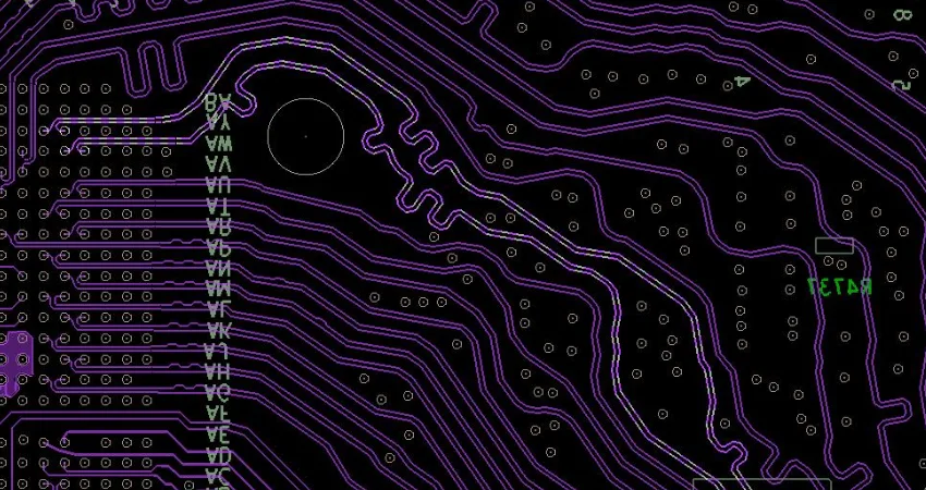
Trace layout determines whether high frequency signals arrive intact or degraded beyond recognition. Every geometric decision—width, thickness, spacing, orientation—affects impedance, loss, and coupling. Unlike low-frequency routing where traces simply connect points, HF trace layout requires deliberate optimization of electromagnetic characteristics.
This guide provides practical techniques for laying out high frequency traces that maintain signal integrity throughout the signal path.
HILPCB manufactures high frequency PCBs with precision trace geometry (±10% width tolerance, tighter on request) and controlled impedance (±5% standard) to preserve your carefully designed trace layouts.
Trace Width Calculation for Target Impedance
Trace width is the primary variable controlling characteristic impedance. Calculating correct width requires understanding the relationship between geometry, materials, and impedance for your specific stackup configuration.
At HILPCB, our impedance calculation service provides optimized trace widths for your target impedance, accounting for actual material Dk, copper weight, and manufacturing tolerances.
Microstrip Impedance Relationships
For outer layer traces above a ground plane, impedance decreases as trace width increases. The relationship also depends on dielectric thickness (distance to reference plane), dielectric constant (Dk), and copper thickness.
- Wider trace → Lower impedance
- Thicker dielectric → Higher impedance
- Higher Dk → Lower impedance
- Thicker copper → Slightly lower impedance (minor effect)
Width Calculation Approach
Never calculate trace width by hand—use field solvers or validated calculators. Online calculators provide rough estimates; dedicated tools like Polar SI9000 or built-in EDA calculators give production-ready values. Input your actual stackup parameters: material Dk at operating frequency, exact dielectric thickness, copper weight, and surface finish.
Typical Width Ranges
For common impedance targets on standard stackups:
| Target Z | 4-mil dielectric | 8-mil dielectric |
|---|---|---|
| 50Ω | ~7 mils | ~15 mils |
| 75Ω | ~4 mils | ~8 mils |
| 90Ω diff | ~4/8 mils | ~6/12 mils |
| 100Ω diff | ~4/10 mils | ~5/14 mils |
These are approximate—calculate exact values for your specific materials.
Manufacturing Tolerance Impact
Trace width variation directly affects impedance. A ±1 mil width tolerance on a 6-mil trace creates ±17% geometry variation, translating to approximately ±5-8% impedance variation. For tighter impedance control, use wider traces (lower percentage variation) or specify tighter width tolerance (adds cost). HILPCB standard tolerance is ±10% width (±0.5 mil minimum); tighter tolerances available for critical applications.
Trace Thickness and Copper Weight Selection
Copper thickness affects both impedance and current-carrying capacity. At high frequencies, skin effect limits the benefit of thicker copper for signal traces but remains important for power distribution.
HILPCB offers copper weights from 0.5 oz to 6 oz (and heavier for specialty applications), with consistent plating thickness critical for high frequency performance.
Standard Copper Weights
- 0.5 oz (17 μm): Fine-pitch routing, high density, lower current
- 1 oz (35 μm): General purpose, balanced performance
- 2 oz (70 μm): Higher current, power distribution
- 3+ oz: Heavy current, power electronics
Skin Effect Considerations
At high frequencies, current concentrates in a thin surface layer. Skin depth in copper: ~2.1 μm at 1 GHz, ~0.66 μm at 10 GHz. Once copper thickness exceeds 3-4 skin depths, additional thickness provides no benefit for AC signals. For high frequency signal traces, 0.5-1 oz copper is typically adequate.
Plating Thickness Variation
Electroplated copper adds thickness during manufacturing. Standard plating adds 0.5-1 oz equivalent. This additional copper changes impedance slightly and must be accounted for in calculations. Specify finished copper weight rather than base copper weight for accurate impedance.
Roughness and Loss
Copper surface roughness increases high frequency loss. Standard electrodeposited copper has roughness (Rz) of 3-5 μm. Low-profile copper options reduce roughness to 1.5-2 μm, reducing loss by 20-40% at frequencies above 10 GHz. For critical high frequency applications, specify low-profile foil.
Trace Geometry Quick Reference
Differential Pair Layout Requirements
Differential signaling dominates high-speed digital interfaces. Proper differential pair layout maintains the balance essential for common-mode noise rejection and EMI control.
At HILPCB, differential pairs receive automated DRC verification for spacing, length matching, and symmetry to ensure balanced performance.
Coupling Geometry
Differential pairs can be edge-coupled (side by side) or broadside-coupled (vertically stacked). Edge coupling is standard for most applications, offering easier routing and inspection. Broadside coupling saves horizontal space but requires precise layer registration.
- Edge-coupled: Traces side by side on same layer
- Broadside-coupled: Traces stacked on adjacent layers
Spacing and Impedance
Differential impedance depends on both single-ended impedance and coupling between traces. Tighter spacing increases coupling, reducing differential impedance. The relationship: Zdiff = 2 × Z0 × (1 - k), where k is coupling coefficient (typically 0.1-0.3).
For 100Ω differential with 50Ω single-ended traces, coupling coefficient should be near zero (wide spacing). For 85Ω differential from 50Ω traces, moderate coupling is needed (tighter spacing).
Length Matching Requirements
Differential pair traces must match lengths to maintain signal balance. Skew (length difference) converts differential signals to common-mode, degrading receiver performance. Matching requirements by data rate:
- < 1 Gbps: ±50 mils adequate
- 1-5 Gbps: ±20 mils typical
- 5-15 Gbps: ±5 mils required
15 Gbps: ±2-3 mils critical
Symmetry Considerations
Beyond length matching, maintain symmetric routing. Both traces should see identical environments: same reference plane, same via count, same bend structure. Asymmetric routing creates imbalance even with matched lengths.
Ground Reference and Return Path Layout
High frequency return current flows directly beneath the signal trace, not through arbitrary ground paths. Proper ground reference layout is essential for signal integrity and EMI control.
HILPCB engineering reviews verify return path continuity for high frequency designs, identifying potential issues before manufacturing.
Return Current Behavior
At high frequencies, return current takes the path of minimum inductance, which is directly beneath the signal. The current density mirrors the signal trace position, spreading only slightly wider than the trace itself. This path minimizes loop area and stored magnetic energy.
Reference Plane Requirements
High frequency signals need solid reference planes without breaks. Any gap, slot, or split forces return current to detour, creating inductance. This inductance distorts signals and increases EMI. Design requirements:
- No splits beneath HF traces
- No cutouts or voids under signal paths
- Continuous copper for minimum 3× trace width on each side
- Solid stitching via fences around plane edges
Plane Layer Selection
Ground planes make better references than power planes. Ground is more stable (no switching noise) and connects directly to component grounds. When power plane must serve as reference, add sufficient decoupling to stabilize the plane voltage.
Via Stitching for Return Path
When signals change layers, return current must also transition. Place ground vias adjacent to signal vias to provide return path continuity. For differential pairs, place ground vias between and beside the signal vias. Spacing should be less than λ/10 at the highest frequency of interest.
Component Placement for Optimal Trace Layout
Component placement largely determines trace layout quality. Poor placement forces long routes, excessive layer transitions, and routing congestion. Strategic placement simplifies high frequency trace layout.
At HILPCB, our DFM review includes placement assessment for signal flow optimization and routing efficiency.
Signal Flow Orientation
Arrange components to create natural signal flow. Place signal source and destination close together to minimize trace length. Orient components so signal pins face each other, reducing routing complexity. Group related components (driver, line, receiver) to contain high frequency signals in small areas.
Grouping Strategy
Group components by function and frequency:
- RF/analog section separate from digital
- High-speed interfaces clustered together
- Clock generation isolated from sensitive receivers
- Power supplies at board edges or separate areas
Placement for Differential Pairs
For differential interfaces, align source and destination connectors to enable straight, parallel routing. Avoid placement that forces pairs to navigate around obstacles or make unnecessary turns. Equal pin-to-trace distances at both ends simplify length matching.
Decoupling Capacitor Placement
Place decoupling capacitors close to IC power pins—within 100 mils for high frequency effectiveness. Route power connections through capacitors, not around them. Use multiple via connections to reduce capacitor inductance. For critical ICs, place smallest capacitors closest to pins.
Manufacturing Considerations for HF Trace Layout
Design choices must align with manufacturing capabilities. Understanding process limits prevents layouts that cannot be fabricated accurately or cost-effectively.
HILPCB provides manufacturing capability documentation and DFM feedback to ensure your trace layout aligns with production processes.
Minimum Geometry Rules
Standard high frequency capable processes support:
- Minimum trace width: 3-4 mils (process dependent)
- Minimum spacing: 3-4 mils (same as width)
- Minimum annular ring: 3-4 mils
- Registration tolerance: ±1-2 mils
Pushing below these limits increases cost and defect risk. Design with comfortable margins when performance allows.
Etch Factor Considerations
Chemical etching removes copper at an angle, creating trapezoidal trace cross-section rather than rectangular. Thicker copper exacerbates this effect. Trace width at top differs from width at base. Impedance calculations should account for average width or use field solvers that model trapezoidal geometry.
Panelization Effects
Large panels may show trace width variation across the panel due to uneven etching. For critical impedance, place test coupons at multiple panel positions. HILPCB uses statistical process control to maintain consistent etching across panels.
Surface Finish Impact
Surface finish affects trace dimensions slightly. ENIG adds nickel/gold to copper surface. Immersion tin/silver add thinner coatings. Account for finish thickness in critical applications. For best high frequency performance, immersion silver offers low loss and consistent thickness.
FAQ
Why can't high frequency trace layout be reduced to just trace width and spacing rules?
Because line geometry is only one part of the channel. Dielectric thickness, reference-plane continuity, copper roughness, via transitions, and surface finish all influence impedance, loss, and EMI. If those factors are not locked with the routing rules, a board can still miss its signal-integrity target even when the nominal width and spacing look correct.
Is differential-pair length matching enough by itself?
No. Differential pairs also need stable coupling, symmetric routing environments, consistent reference planes, and well-controlled layer transitions. Two traces can be perfectly length-matched and still behave poorly if one side sees a different return path or a different via structure.
Why is return-path continuity so important when a high frequency signal changes layers?
Because the return current must transition with the signal. If there is no nearby reference-via path, the return current detours, increasing loop inductance, reflections, and EMI risk. That is why signal vias and ground stitching vias need to be considered as one structure, not as separate details.
What is the most valuable layout optimization to make before routing starts?
Place source, connector, receiver, and clock-related components so the intended signal flow is short and direct, with continuous reference planes available underneath. Good placement removes routing compromises early and usually improves both signal quality and manufacturability.
Related High Frequency Routing Topics
- High Frequency PCB Routing Design: Complete HF routing methodology
- Routing Clearance in HF PCB: Spacing rules for crosstalk control
- Corner Routing for High Frequency PCB: Bend and corner optimization
- Trace Length Control in HF PCB: Length matching and delay management
- Routing Discontinuity in HF PCB: Managing impedance transitions
HILPCB Trace Layout Services
HILPCB delivers the manufacturing precision your high frequency trace layouts require:
Impedance Engineering: Pre-build trace width calculation, stackup optimization, and impedance verification for your specific requirements.
Geometry Control: Precise trace width (±10% standard, tighter available), consistent copper thickness, and accurate registration for reliable high frequency performance.
Material Options: Full range of copper weights, low-profile foil options, and surface finishes optimized for high frequency applications.
Verification: 100% TDR testing on controlled impedance traces with detailed reports documenting compliance.
From prototypes through production, HILPCB maintains consistent trace geometry for high frequency applications.
Contact HILPCB for trace layout review and manufacturing quotation.