
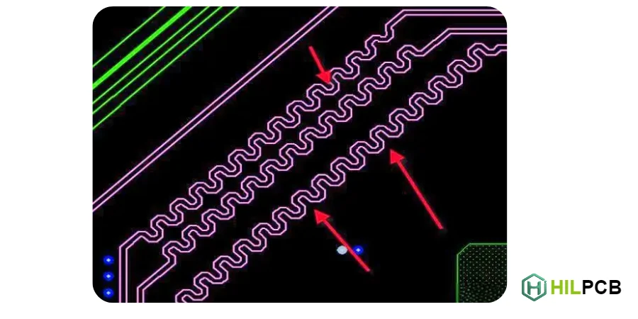
Trace length directly determines signal arrival time. In high frequency systems, microseconds matter—actually, picoseconds matter. When signals must arrive simultaneously, maintain specific timing relationships, or meet setup and hold requirements, trace length control becomes a fundamental design discipline.
This guide provides practical techniques for managing trace length in high frequency PCBs, from understanding delay requirements to implementing precise length matching.
HILPCB manufactures high frequency PCBs with the dielectric consistency (±5% thickness tolerance) required for predictable propagation delay, supporting differential skew requirements down to ±5 ps.
Why Trace Length Matters at High Frequencies
At high frequencies, physical trace length translates directly to electrical delay. Signals don't arrive instantaneously—they propagate at finite velocity determined by the dielectric material.
At HILPCB, our engineering team validates length requirements and provides propagation delay calculations based on actual stackup parameters.
Propagation Velocity
Signals in PCB traces travel at roughly half the speed of light, varying with dielectric constant. In FR-4 microstrip: approximately 6 inches/ns (140-150 ps/inch). In FR-4 stripline: approximately 5.5 inches/ns (170-180 ps/inch). Lower Dk materials provide faster propagation.
Length to Delay Conversion
Every inch of trace adds delay. For FR-4 microstrip at 145 ps/inch:
- 1 inch = 145 ps
- 100 mils = 14.5 ps
- 10 mils = 1.45 ps
Small length differences create measurable timing differences at high data rates.
When Length Control Matters
Critical applications include:
- Differential pairs (skew requirements)
- Parallel buses (data-to-strobe timing)
- Multi-lane interfaces (lane-to-lane alignment)
- Clock distribution (matched arrival times)
- Source-synchronous interfaces (setup/hold timing)
Consequences of Length Mismatch
Inadequate length control causes timing failures, reduced noise margin, data errors, and failed compliance testing. The severity depends on data rate—a 50 ps timing error that's invisible at 1 Gbps causes bit errors at 25 Gbps.
Differential Pair Length Matching Requirements
Differential pairs require matched trace lengths to maintain signal balance. Length mismatch (skew) converts differential signals to common-mode, degrading performance.
HILPCB provides differential pair verification with length matching reports documenting compliance with your specifications.
Skew Effects
When differential traces have unequal lengths, the signals arrive at different times. This timing offset appears as common-mode noise at the receiver, reducing common-mode rejection and potentially causing detection errors.
Data Rate vs. Skew Tolerance
Higher data rates demand tighter matching:
| Data Rate | Unit Interval | Typical Max Skew |
|---|---|---|
| 1 Gbps | 1000 ps | 50-100 ps (35-70 mils) |
| 5 Gbps | 200 ps | 15-20 ps (10-15 mils) |
| 10 Gbps | 100 ps | 5-10 ps (3-7 mils) |
| 25 Gbps | 40 ps | 2-4 ps (1-3 mils) |
Interface-Specific Requirements
Standard specifications define skew limits:
- USB 3.0: ±15 ps maximum
- PCIe Gen 4: ±5 ps maximum
- HDMI 2.1: ±10 ps maximum
- 100G Ethernet: ±5 ps maximum
Length to Delay Conversion (FR-4 Microstrip)
Multi-Lane and Bus Length Matching
Parallel interfaces with multiple signals must maintain timing alignment between all lanes. Different matching strategies apply depending on interface architecture.
At HILPCB, our DFM review validates multi-lane length matching against your interface specifications.
Source-Synchronous Interfaces
In source-synchronous architectures, data travels with its clock (strobe). Data must arrive within setup and hold windows relative to strobe edges. Matching requirements:
- Data-to-strobe matching: Tight (defines sampling window)
- Lane-to-lane matching: Moderate (receiver realigns)
- Byte lane grouping: All signals in byte group match to common strobe
Example: DDR4/DDR5 Memory
DDR interfaces group 8 data bits with a strobe (DQS). Requirements:
- DQ-to-DQS matching within byte lane: ±5 ps typical
- Address/command-to-clock: ±25 ps typical
- Clock-to-clock: ±5 ps for differential clock
Multi-Gigabit SerDes
High-speed serial links (PCIe, USB, Ethernet) use clock recovery—the receiver extracts timing from data transitions. This relaxes inter-lane matching but requires:
- Intra-pair matching: Tight (differential skew limits)
- Lane-to-lane matching: Moderate (compensated by receiver)
- Reference clock distribution: Matched to all transmitters
Matching Hierarchy
Apply tightest matching to most timing-critical relationships:
- Intra-pair (within differential pair): Tightest
- Intra-byte (within byte lane): Tight
- Inter-byte (between byte lanes): Moderate
- Inter-channel (between interfaces): Relaxed
Serpentine Routing Techniques
Serpentine routing (also called meander or accordion routing) adds length to shorter traces, achieving length matching without changing the physical routing path.
HILPCB manufacturing accurately reproduces serpentine geometries; our DFM review verifies serpentine rules are appropriate for your frequency.
Basic Serpentine Structure
Serpentine consists of alternating parallel segments connected by bends. Key parameters:
- Amplitude: Height of each meander
- Spacing: Distance between parallel segments
- Segment count: Number of meanders
Design Rules for Effective Serpentine
Poor serpentine design creates coupling between adjacent segments, degrading signal quality. Follow these guidelines:
- Amplitude ≥ 3× trace width (minimum)
- Segment spacing ≥ 3× trace width
- Prefer larger spacing when possible
- Keep total serpentine compact
- Place close to the length mismatch source
Serpentine Placement
Place serpentine immediately after the length mismatch occurs rather than accumulating at the end of the trace. For corner-induced mismatch, add serpentine after the corner. For component placement mismatch, add serpentine near the shorter path's source.
Frequency Limitations
At very high frequencies (>10 GHz), serpentine segments can self-couple, creating resonances. For multi-Gbps signals, consider increasing segment spacing or using alternative length matching approaches like component placement optimization.
Propagation Delay Calculation
Accurate delay calculation enables precise length matching and timing analysis. Delay depends on material properties and trace structure.
HILPCB provides propagation delay calculations based on actual stackup parameters for timing-critical designs.
Microstrip Delay
For outer layer traces with reference plane below:
Delay ≈ 85 × √(0.475 × Dk + 0.67) ps/inch
For FR-4 (Dk ≈ 4.3): Delay ≈ 140-150 ps/inch
Stripline Delay
For traces between two reference planes:
Delay ≈ 85 × √Dk ps/inch
For FR-4 (Dk ≈ 4.3): Delay ≈ 170-180 ps/inch
Material Impact
Lower Dk materials provide faster propagation:
| Material | Dk | Microstrip Delay |
|---|---|---|
| FR-4 | 4.3 | ~145 ps/inch |
| Megtron 6 | 3.6 | ~130 ps/inch |
| RO4350B | 3.48 | ~128 ps/inch |
| RT/duroid | 2.2 | ~105 ps/inch |
Delay Matching Considerations
When matching delay (not just length), account for different propagation velocities on different layers or materials. A signal on microstrip and a signal on stripline require different physical lengths for equal delay.
Manufacturing Impact on Length Control
Manufacturing variations affect actual trace length and propagation delay. Understanding these effects enables appropriate design margins.
HILPCB maintains tight process control for consistent length and delay characteristics across production.
Dielectric Thickness Variation
Dielectric thickness affects propagation velocity. Standard tolerance of ±10% creates proportional delay variation. For critical applications, HILPCB offers ±5% dielectric control.
Dk Variation
Dielectric constant varies with material batch, panel position, frequency, and temperature. Specify Dk tolerance requirements for timing-critical applications.
Fiber Weave Effect
In woven glass substrates, traces aligned with glass bundles see different effective Dk than traces over resin channels. This creates delay variation between adjacent traces routed in different directions relative to the weave. Mitigation strategies:
- Rotate trace angles relative to weave
- Use spread glass materials
- Specify low-weave-effect materials for critical timing
Registration Effects
Layer-to-layer misregistration can affect differential pair balance if traces are not symmetrically positioned. HILPCB registration of ±15-25 μm minimizes this effect.
Related High Frequency Routing Topics
- High Frequency PCB Routing Design: Complete HF routing methodology
- Trace Layout for High Frequency PCB: Geometry optimization strategies
- Routing Clearance in HF PCB: Spacing rules for crosstalk control
- Corner Routing for High Frequency PCB: Bend and corner optimization
- Routing Discontinuity in HF PCB: Managing impedance transitions
HILPCB Length Control Services
HILPCB delivers the manufacturing consistency your timing-critical designs require:
Dielectric Control: ±5% thickness tolerance available for consistent propagation delay across production lots.
Material Expertise: Dk-characterized materials with documented propagation velocity for accurate delay calculations.
Verification: Length matching validation and differential skew measurement through TDR testing.
Process Consistency: Statistical process control ensures board-to-board delay consistency within specified tolerances.
From prototypes through production, HILPCB maintains the precision required for timing-critical high frequency applications.
Contact HILPCB for length control review and manufacturing quotation.