
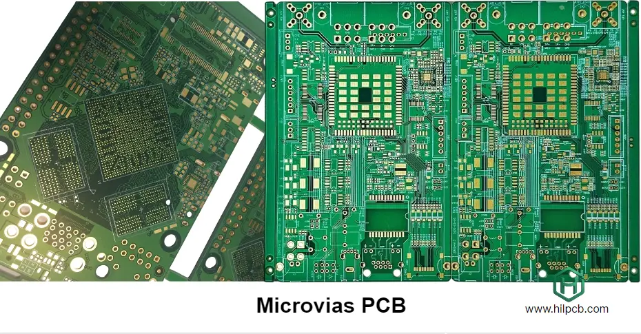
At the crest of AI and HPC, advanced AI chips, HBM, and Chiplet packaging are evolving at unprecedented speed. The “heart” of these systems—AI chip interconnect and IC substrate PCBs—has reached a new level of complexity. When a single substrate can be worth thousands of dollars and a tiny defect can trigger catastrophic loss, traditional manufacturing approaches are no longer enough. A powerful, end-to-end Traceability/MES system is not a nice-to-have—it becomes the core enabler of performance, reliability, and yield. From the perspective of a power integrity engineer, this article explains why Traceability/MES is the key to managing AI substrate manufacturing challenges.
Why do AI substrates demand such strict process control?
Modern AI accelerators using CoWoS, EMIB, and other 2.5D/3D packaging integrate system-level functions into a single package. This is not “just a PCB”—it’s a highly integrated micro-system. Strict process control is required because:
- Extreme interconnect density: RDL line/space can reach ~10 μm or below—far beyond traditional PCBs. Small registration errors, etch non-uniformity, or plating defects can create opens/shorts in high-speed channels, directly impacting HBM↔SoC communication.
- Severe PI challenges: transient currents can reach hundreds of amps with high dI/dt, demanding ultra-low PDN impedance. Embedded capacitance structures, dense decoupling, and thick copper must be manufactured precisely; plating thickness issues or delamination can degrade PDN and cause voltage droop and compute instability.
- Complex thermal requirements: 1000W+ is common. Substrates integrate Copper Coin and Thermal Vias to move heat efficiently to the heatsink. Manufacturing accuracy and reliability of these structures determine thermal performance.
- Heterogeneous materials and structures: hybrid stackups (e.g., ABF) balance electrical performance and cost. CTE mismatch across materials plus large package size (up to 100 mm × 100 mm) makes Warpage control a major challenge.
In such a complex chain, tiny process fluctuations can amplify and scrap an expensive module. That’s where Traceability/MES becomes essential.
How Traceability/MES becomes the foundation of HDI manufacturing
Traceability/MES is an integrated manufacturing management system that brings unprecedented transparency and control to complex electronics manufacturing. It combines two complementary layers:
- Traceability: the system’s “memory”. It assigns a unique serial number to each PCB/substrate and records its full lifecycle: material and chemistry lots, equipment IDs, operator/time, and key process parameters (temperature, pressure, exposure energy, etc.). This per-unit trace is the foundation for problem-solving and continuous improvement.
- MES: the system’s “brain and nervous system”. It executes production plans, turns design data (Gerber, ODB++) into machine instructions, enforces process flows/specs, and compares real-time sensor/equipment data against limits. Deviations can trigger alarms or even line stops to prevent batch defects.
For AI substrates, a strong MES—like the system deployed by Highleap PCB Factory (HILPCB)—ensures every IC Substrate PCB is built to spec. It converts abstract design requirements (impedance, line width) into concrete, controlled, traceable manufacturing parameters—bridging design and reality.
HILPCB AI substrate & HDI manufacturing capability matrix
| Parameter | HILPCB standard capability | HILPCB advanced capability | Value for AI substrates |
|---|---|---|---|
| Max layer count | 32 layers | 56 layers | Supports complex power and signal routing needs |
| Min line/space | 2/2 mil (50/50 µm) | 0.4/0.4 mil (10/10 µm) | Enables RDL routing for dense interfaces like HBM |
| Laser drill min diameter | 50 µm | 25 µm | Supports high-density Microvia stacking |
| Impedance control accuracy | ±8% | ±5% | Protects signal quality for PCIe 6.0 / HBM3e |
| Material options | High-Tg FR-4, Rogers | Megtron 6/7, ABF, Ceramic | Meets different performance and cost targets |
How MES accelerates iteration and validation in NPI
NPI—especially NPI EVT/DVT/PVT—is a race against time for fast-iterating AI hardware. In traditional NPI flows, root-cause analysis after a failure can take days or weeks, requiring manual record digging and cross-team coordination. With integrated Traceability/MES, the loop changes:
- Faster issue localization: if HBM links show errors in DVT, engineers can pull the complete manufacturing history instantly. In a few clicks, they can see whether the affected boards share an ABF lot or a specific lamination machine—compressing analysis from days to hours.
- Data-driven optimization: EVT pilot builds often run detailed electrical validation using Flying probe test. MES binds flying-probe results (per-net resistance/capacitance measurements, etc.) to manufacturing parameters (etch time, plating current). Analysis reveals how small process tweaks change electrical outcomes, enabling fast optimization before DVT/PVT.
- Design-manufacturing co-optimization: real manufacturing deviation data (e.g., actual line width vs design) can be fed back to design engineers, enabling compensation based on true capability. This DFM closed loop is key to accelerating NPI EVT/DVT/PVT.
How MES enables precise SI control for high-speed channels
For AI accelerators, SoC↔HBM links are the lifeline, carrying Tb/s traffic. Any small SI issue—impedance mismatch, crosstalk, loss—can create data errors and drag system performance down.
Traceability/MES turns SI from a “design target” into a “controllable manufacturing outcome”:
- Material lot management: Dk/Df vary slightly across lots. MES records material lots per board and can use supplier test data to fine-tune parameters (etch compensation, etc.) so impedance stays inside tight ±5% windows.
- Closed-loop geometry control: line width/thickness and spacing to reference planes define impedance. MES integrates AOI and X-Ray metrology, monitors per-layer line width, and adjusts downstream steps (e.g., etch) to close the loop—critical for High-Speed PCB.
- Plating uniformity monitoring: differential pairs require highly matched copper thickness. By monitoring bath chemistry, current density, time, and cross-section data, MES keeps plating uniform across the panel and across lots, protecting differential symmetry.
This shifts SI assurance from “after-the-fact testing” to “process-built quality”, improving yield and consistency for advanced substrates.
🔄 Traceability / MES closed-loop manufacturing data system
Full-chain traceability and automated process optimization—from design inputs to finished goods.
Import Gerber and BOM to establish a digital traceability baseline and process spec archive.
MES captures SMT placement parameters, zone profiles, and material lot info in real time.
SPI/AOI/X-Ray results are linked to serial numbers automatically for precise defect containment.
Store flying-probe and ICT electrical data in MES to create per-board lifecycle records.
Use big-data analysis to detect line drift and close the loop via upstream corrections.
How PI and thermal management benefit from traceability
From a PI engineer’s view, PDN and thermal are tightly coupled on AI substrates, and Traceability/MES matters for both.
For PI, low-impedance PDN depends on precise fabrication. For example, via-in-pad copper fill quality directly affects via resistance. MES ensures fill parameters—chemistry concentration, plating time—are followed and recorded. In SMT assembly, the system verifies decoupling capacitor type/value against BOM and records exact placement. If PI issues appear later, engineers can trace whether the root is a capacitor lot, a placement deviation, or a specific process drift.
For thermal, traceability is equally critical. If a design uses embedded Copper Coin, MES records lamination pressure/temperature profiles to ensure void-free bonding and minimum thermal resistance. If thermal interface materials (TIM) are applied, MES can record dispense weight/thickness/location to keep thermal performance consistent and prevent throttling under load.
Closing the loop: from flying probe test to ICT/FCT
Test is the last quality barrier, but it shouldn’t be isolated. Traceability/MES integrates test data across stages into a closed-loop quality system:
- Flying probe test: in samples and small batches, flying probe provides fixtureless flexibility for opens/shorts and basic electrical checks. MES binds the report to the board’s unique serial number.
- Fixture design (ICT/FCT): in volume, customized fixtures improve efficiency and coverage. MES records not only pass/fail, but also measured component parameters (R/C values) and FCT logs.
The value: if ICT/FCT detects a trend (e.g., resistance creeping high), quality engineers can trace all affected boards in Traceability/MES and find the common factors—machine, copper lot, chemistry batch—then apply corrective actions before customer complaints happen.
HILPCB one-stop assembly advantages
Unified Traceability/MES
Seamless data handoff from PCB fabrication to SMT assembly for end-to-end traceability and consistent quality.
DFM/DFA co-analysis
Engineers engage early to co-optimize the design and ensure manufacturability and assembly feasibility.
Supply chain governance
Strict component sourcing and traceability to block counterfeit parts and protect supply security.
Advanced test capability
Full test coverage from AOI and X-Ray to ICT/FCT, including professional Fixture design (ICT/FCT) services.
The core value of Traceability/MES in Turnkey PCBA
Turnkey PCBA—a single supplier covering PCB fabrication, component sourcing, SMT assembly, and test—is increasingly preferred in AI hardware. In this model, a unified Traceability/MES is the key to success.
When PCB fabrication and assembly are done by separate factories, the information chain often breaks: the assembler lacks fabrication parameters, and the PCB factory can’t see assembly performance. A true Turnkey PCBA provider like HILPCB uses a unified Traceability/MES to connect everything:
- Seamless data flow: PCB manufacturing history (materials, impedance test data, etc.) flows into the SMT assembly line. Placement machines can even fine-tune parameters based on per-board warpage measurements to improve BGA yield.
- Complete lifecycle record: from bare board steps to component lots, reflow profiles, and functional test results—everything is stored in one database tied to the product serial number, enabling unmatched QA and after-sales traceability.
- Clear ownership: when issues occur, there is no finger-pointing between vendors. Root-cause localization becomes faster and responsibility is clear, enabling faster resolution.
For AI programs with tight schedules and complex supply chains, choosing a Turnkey PCBA partner with a strong MES means outsourcing manufacturing complexity to specialists—so teams can focus on chips and algorithms.
What new challenges will future AI manufacturing place on Traceability/MES?
As Chiplet, 3D stacking, and CPO mature, manufacturing complexity will keep rising—raising the bar for Traceability/MES:
- From 2D to 3D traceability: track not only substrates, but each chiplet’s wafer position, test results, bonding location on the substrate, and process parameters—extending traceability into 3D space.
- AI-powered predictive maintenance: next-gen MES will integrate machine learning to predict quality risks and equipment failure, shifting from reactive to proactive control.
- Broader ecosystem integration: deeper integration with upstream/downstream systems (material suppliers, chip designers, end customers) to increase value-chain transparency and jointly manage quality and security risk.
HILPCB continues to invest in Traceability/MES upgrades to meet leading-edge requirements and drive AI hardware innovation with customers.
FAQ
Why Is Traceability/MES So Important for AI Substrate Manufacturing?
AI substrate manufacturing combines high density, tight electrical tolerances, extreme thermal demands, and complex material interactions. Traceability/MES provides the control layer needed to connect each board to its material history, process conditions, inspection data, and test outcomes.
How Does Traceability/MES Help During NPI?
During NPI, teams need fast feedback between design, manufacturing, and test. Traceability/MES speeds that loop by linking failures and process deviations back to specific parameters, lots, and build records, which makes root-cause analysis and engineering iteration much faster.
Why Does Traceability/MES Matter in Turnkey PCBA?
In turnkey PCBA, PCB fabrication, sourcing, assembly, and testing must work as one coordinated flow. A unified Traceability/MES system reduces information breaks between stages, preserves full lifecycle records, and makes responsibility and problem resolution much clearer.
What New Challenges Will Future AI Hardware Create for Traceability/MES?
As AI hardware moves toward chiplets, 3D packaging, and more complex supply chains, Traceability/MES will need deeper data integration, more granular device-level tracking, and more predictive quality control. The system must evolve from recording history to actively guiding manufacturing decisions.
Conclusion
For AI chip interconnect and IC substrate PCBs—high risk and high value—manufacturing is no longer just “building to drawings”. It’s a science requiring precise control, massive data, and continuous optimization. Traceability/MES is the nervous system that turns target performance into reliable physical reality through end-to-end traceability, real-time process control, and closed-loop feedback.
From accelerating NPI EVT/DVT/PVT, to protecting SI, to powering Turnkey PCBA, the value of Traceability/MES spans the full lifecycle. Choosing a manufacturing partner that treats Traceability/MES as a core quality culture is one of the smartest decisions an AI hardware team can make.