
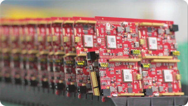
Executing rapid-turn Surface Mount Technology (SMT) assembly during New Product Introduction (NPI) requires balancing tight project schedules with strict zero-defect quality controls. As industrial and commercial electronic assemblies integrate high-density micro-BGAs ($0.4\text{ mm} - 0.5\text{ mm}$ pitch), ultra-miniature passives ($0201$ and $01005$), and multi-pad Bottom-Terminated Components (QFNs, DFNs, MOSFETs), the margin for manufacturing process variation shrinks dramatically. Empirical production yield analyses establish that more than $65%$ of all surface-mount assembly defects—bridging, solder beading, tombstoning, and open joints—originate directly during the solder paste stencil printing stage.
In full turnkey PCB assembly, the manufacturing partner manages the end-to-end supply and assembly chain: bare board fabrication, authorized electronic component procurement, precision laser stencil fabrication, automated pick-and-place, multi-zone reflow soldering, and automated optical and X-ray inspection. To ensure initial prototype bring-up builds transition smoothly to mass production, engineers must control stencil aspect ratios, design partitioned ground apertures to mitigate BGA voiding under IPC-A-610 Class 3, and enforce automated First Article Inspection (FAI) before batch production.
| Process Variable | Standard Commercial SMT (IPC Class 2) | High-Reliability NPI SMT (IPC Class 3) | Primary Process Control |
|---|---|---|---|
| Minimum Stencil Area Ratio (AR) | $\ge 0.66$ (Standard laser-cut foil) | $\ge 0.66$ (Nano-coated or electroformed foil) | IPC-7525 paste transfer efficiency calculation |
| BGA / BTC Solder Voiding Limit | $\le 25%$ total projected ball area | $\mathbf{\le 15%}$ total void area ($\le 10%$ single void) | 3D AXI oblique-angle computed tomography |
| Component Value Verification | Visual bill-of-materials sampling | $100%$ automated LCR bridge testing on first board | Automated First Article Tester against CAD netlist |
| Component Sourcing Traceability | Commercial distributor inventory | $100%$ authorized franchise distribution with CoC | AS6081 / IDEA-STD-1010 anti-counterfeit protocol |
| Reflow Atmospheric Control | Ambient air convection reflow | Nitrogen ($N_2$) inert purge ($O_2 < 500\text{ ppm}$) | Wetting enhancement and intermetallic control |
SMT Stencil Design, Aperture Reduction, and Area Ratio Matrix
Solder paste transfer from stencil apertures onto PCB copper pads is governed by surface tension and fluid dynamics. For complete paste release, the adhesion force between the paste and the copper pad must exceed the frictional shear force between the paste brick and the internal aperture sidewalls.
       IPC-7525 STENCIL APERTURE TRANSFER BALANCE
       ===========================================
       Pad Surface Adhesion (L x W) > Sidewall Friction 2*(L + W)*T

       Area Ratio (AR)   = (L x W) / [ 2 x (L + W) x T ]  >= 0.66
       Aspect Ratio      = W / T                           >= 1.50
Stencil Thickness & Aperture Sizing by Component Family
| Component Package | Minimum Pitch / Pad Width | Stencil Foil Thickness ($T$) | Recommended Aperture Geometry | Target Area Ratio (AR) | Stencil Technology Recommendation |
|---|---|---|---|---|---|
| 0805 / 1206 Passives | $\ge 1.27\text{ mm}$ pitch | $125\ \mu\text{m} - 150\ \mu\text{m}$ ($5 - 6\text{ mil}$) | $1:1$ pad match (no reduction) | $\ge 0.90$ | Standard laser-cut stainless steel |
| 0402 Passives / SOIC | $0.50\text{ mm}$ pad width | $120\ \mu\text{m}$ ($4.7\text{ mil}$) | $10%$ area reduction; oblong corners | $\ge 0.75$ | Laser-cut stainless steel |
| 0201 Passives / 0.5mm QFP | $0.25\text{ mm}$ pad width | $100\ \mu\text{m}$ ($4.0\text{ mil}$) | $15%$ area reduction; radius corners | $\ge 0.68$ | Laser-cut with electro-polish |
| 01005 Ultra-Miniature | $0.15\text{ mm}$ pad width | $75\ \mu\text{m} - 80\ \mu\text{m}$ ($3.0\text{ mil}$) | Rounded rectangular; $20%$ reduction | $\ge 0.66$ | Electroformed or Nano-coated foil |
| 0.5 mm Pitch BGA | $0.28\text{ mm}$ round pad | $100\ \mu\text{m}$ ($4.0\text{ mil}$) | Circular aperture reduced by $10%$ | $\ge 0.70$ | Laser-cut + Polymeric Nano-Coating |
| 0.4 mm Pitch BGA / WLCSP | $0.22\text{ mm}$ round pad | $80\ \mu\text{m}$ ($3.2\text{ mil}$) | Square aperture with radiused corners | $\ge 0.66$ | High-precision Electroformed / Nano |
| QFN Exposed Thermal Pad | $3.0\text{ mm} - 6.0\text{ mm}$ square | $100\ \mu\text{m} - 120\ \mu\text{m}$ | Window-pane grid ($35% - 50%$ void) | $\ge 1.20$ | Cross-hatch web pattern ($0.2\text{ mm}$ bridges) |
       Solid Thermal Pad (High Voiding & Solder Floating)    Window-Pane Segmented Aperture (Recommended)
       ==================================================    ============================================
       ┌────────────────────────────────────────────────┐    ┌──────────────┬──────────────┬────────────┐
       │                                                │    │  PASTE BRICK │  PASTE BRICK │ PASTE BRICK│
       │                                                │    ├──────────────┼──────────────┼────────────┤
       │            SOLID 100% PASTE PRINT              │    │  PASTE BRICK │  PASTE BRICK │ PASTE BRICK│
       │                                                │    ├──────────────┼──────────────┼────────────┤
       │                                                │    │  PASTE BRICK │  PASTE BRICK │ PASTE BRICK│
       └────────────────────────────────────────────────┘    └──────────────┴──────────────┴────────────┘
       - Traps volatile outgassing flux solvents             - Open web channels allow solvent gas escape
       - Causes component hydroplaning and pad tilting       - Prevents solder beading; keeps voids < 15%
Why Nano-Coated Stencils Improve NPI First-Pass Yield
Standard laser-cut stainless steel apertures exhibit microscopic striations along their cut edges caused by the laser pulse kerf. Solder paste clings to these micro-grooves, reducing paste transfer efficiency on fine apertures to under $70%$.
- Applying a permanent fluoropolymer or organic phosphonate nano-coating ($2 - 4\ \mu\text{m}$) creates a hydrophobic, oleophobic surface with a contact angle $>110^\circ$.
- Nano-coatings prevent paste particles from adhering to sidewalls, boosting transfer efficiency to $>90%$, eliminating paste bridging between fine-pitch pads, and reducing required underside wipe cycles from every 3 boards to every 15 boards.
BGA & BTC Solder Voiding Mitigation Under IPC-A-610
Solder voids are bubbles of entrapped gas inside the solder joint. While small voids are normal, excessive voiding in Ball Grid Array (BGA) and Bottom-Terminated Component (BTC / QFN) joints decreases mechanical shear strength, accelerates fatigue cracking under thermal cycling, and impairs thermal heat transfer to internal PCB ground planes.
       BGA SOLDER VOID LIMITS (IPC-A-610 / IPC-7095)
       ==============================================
       Class 1 (General Consumer):   <= 30% Total Ball Area Voiding
       Class 2 (Dedicated Business): <= 25% Total Ball Area Voiding
       Class 3 (High Reliability):   <= 15% Total Ball Area Voiding
       Automotive / Under-the-Hood:  <= 10% Total Ball Area Voiding
Root Causes & Process Solutions for Solder Voiding
| Root Cause | Physical Mechanism | Corrective Engineering Action in SMT |
|---|---|---|
| Insufficient Soak Duration | Flux solvent carriers do not fully volatilize before reaching liquidus; trapped gas expands during solder melt | Lengthen reflow soak zone ($150^\circ\text{C} - 190^\circ\text{C}$) to $75 - 90\text{ seconds}$ to achieve complete flux outgassing |
| Excessive Peak Reflow Temp | Flux vehicles decompose chemically and char when overheated ($T > 255^\circ\text{C}$), generating excess carbon gases | Cap peak reflow temperature at $238^\circ\text{C} - 245^\circ\text{C}$ for standard SAC305 lead-free alloys |
| Uncapped Microvia-in-Pad | Drilled microvias inside BGA pads trap atmospheric air beneath the solder sphere during paste reflow | Mandate Via-in-Pad Plated Over (VIPPO / IPC-4761 Type VII): epoxy fill + planar copper cap |
| Solder Paste Oxidation | Solder paste powder expired or exposed to high ambient humidity ($>60%\text{ RH}$); metal oxides release oxygen | Enforce strict $24\text{ h}$ stencil-life limits; store paste at $2^\circ\text{C} - 10^\circ\text{C}$; warm to room temp $4\text{ h}$ before opening |
| Inadequate Wetting Atmosphere | Atmospheric oxygen re-oxidizes molten solder surfaces, impeding bubble escape | Run reflow ovens under an inert Nitrogen ($N_2$) atmosphere with oxygen content controlled $< 500\text{ ppm}$ |
SAC305 Lead-Free Reflow Profile Optimization Window
       Temperature (°C)
          ▲
      250 ┼───────────────────────────────┐ Peak Temp: 240°C - 248°C
          │                              / \
      217 ┼───────────────── Liquidus ──/───\── TAL: 50s - 70s
          │                 ┌──────────┘     \
      190 ┼────────────────/                  \
          │  Preheat Zone │  Thermal Soak     │ Cooling Zone
      150 ┼───────────────┘  60s - 90s        │ -2°C/s to -4°C/s
          │  Ramp: 1°C-3°C/s                  │
       25 ┼───────────────────────────────────┴──────────────► Time (s)
          0               60                 150             220
- Ramp-to-Soak ($25^\circ\text{C} \rightarrow 150^\circ\text{C}$): Slope $1.0^\circ\text{C} - 2.5^\circ\text{C/s}$. Controlled heating prevents solder splatter and thermal shock to ceramic chip capacitors.
- Thermal Soak ($150^\circ\text{C} \rightarrow 190^\circ\text{C}$): Duration $60 - 90\text{ seconds}$. Critical window for equalizing thermal mass between large IC bodies and small passives.
- Time Above Liquidus (TAL, $>217^\circ\text{C}$): Duration $50 - 75\text{ seconds}$. Allows proper intermetallic compound (IMC) formation ($\text{Cu}_6\text{Sn}_5$, thickness $1.0\ \mu\text{m} - 2.5\ \mu\text{m}$) without excessive brittle intermetallic growth.
First Article Inspection (FAI) Verification Sequence
In quick-turn SMT manufacturing, running a full batch without verifying the very first assembled board creates catastrophic scrap risk if a single pick-and-place reel is misloaded or a polarity is inverted.
The First Article Inspection (FAI) protocol pauses the production line after the first board passes the reflow oven until all electrical and mechanical criteria are verified against engineering documentation.
       FIRST ARTICLE INSPECTION (FAI) VERIFICATION SEQUENCE
       ====================================================
       [ STAGE 1 ] Automated LCR Component Measurement & BOM Comparison
       [ STAGE 2 ] 3D Automated Optical Inspection (AOI) Centroid Alignment
       [ STAGE 3 ] 3D Automated X-Ray Inspection (AXI) Hidden Joint Solder Voids
       [ STAGE 4 ] Quality Engineering Sign-Off and Batch Run Authorization
FAI Pass/Fail Acceptance Matrix
| Inspection Stage | Measurement Tool | Inspection Focus & Parameters | Acceptance Threshold |
|---|---|---|---|
| Component Value Verification | Automated Flying-Probe / LCR Bridge | Measures resistance ($R$), capacitance ($C$), inductance ($L$) on all unlabelled passives | Measured value matches BOM nominal value within component tolerance (e.g., $\pm 1%$, $\pm 5%$) |
| Component Placement Offset | 3D AOI (High-Resolution Telecentric) | Placement centroid alignment relative to copper pad centers | Maximum allowable lateral offset $\le 15%$ of component termination width; zero rotation tilt |
| Polarity & Pin 1 Orientation | 3D AOI + Visual Microscopy ($20\times$) | IC Pin 1 notch, diode cathode bands, polarized tantalum capacitor bevels | $100%$ match to PCB silkscreen and schematic design netlist; zero inverted diodes or ICs |
| Solder Joint Meniscus Fillet | 3D AOI (Multi-Angle Color Lighting) | Heel, toe, and side wetting fillets under IPC-A-610 Class 3 | Solder fillet covers $\ge 75%$ of lead height; zero tombstoning, dewetting, or bridging |
| Hidden Joint & BGA Inspection | 3D AXI (Oblique Angle Computed Tomography) | Ball shape, bridging, head-in-pillow (HiP) defects, voiding ratio | Total void area $< 15%$ per ball; zero bridging; spherical ball shape without collapse asymmetry |
Turnkey BOM Sourcing & Counterfeit Prevention Protocol
Component authenticity and lifecycle availability are the cornerstone of successful turnkey PCB assembly. Procuring electronic components through unverified broker channels risks receiving refurbished, remarketed, or counterfeit parts that cause intermittent field failures.
       SUPPLY CHAIN INTEGRITY & TRACEABILITY PROTOCOL
       ==============================================
       Tier 1: Direct Franchise Distribution (DigiKey, Mouser, Arrow, Avnet, Future)
               -> 100% Factory Sealed Packaging with Manufacturer Certificate of Conformance (CoC)

       Tier 2: Hard-to-Find / Long Lead-Time Secondary Procurement
               -> Sourced via ISO 9001 / AS6081 Certified Authorized Stocking Distributors
               -> Mandatory Testing: Decapsulation, X-Ray Die Verification, XRF Lead Metallurgy
Sourcing & Verification Workflow for NPI Builds:
- Automated BOM Scrubbing: During the initial DFM intake, our engineering software checks every component against real-time global inventory APIs, identifying End-of-Life (EOL), Not Recommended for New Designs (NRND), and long lead-time components before order placement.
- Form-Fit-Function (FFF) Equivalents: If a component has an extended factory lead time (e.g., 26 weeks), our engineering team proposes drop-in Pin-Compatible Alternates (PCA), verifying voltage tolerances, package footprint dimensions, and temperature ratings for customer approval.
- Moisture-Sensitive Device (MSD) Management: All active ICs are tracked under IPC/JEDEC J-STD-033. Components rated MSL 3, 4, 5, or 6 that exceed their allowable floor life are baked in calibrated nitrogen dry cabinets ($125^\circ\text{C}$ for $24\text{ hours}$) before SMT placement to eliminate popcorn delamination during reflow.
Production Engineering Data Package Requirements
To ensure accurate machine programming, tooling setup, and automated inspection generation, your NPI handoff package should include the following core deliverables:
1. Fabrication & Paste Mask Gerber Data
- Complete RS-274X or ODB++ archive including copper, solder mask, silkscreen, drill files, and dedicated Paste Mask (Solder Paste) Layers (
.GTP/.GBP). - Stencil thickness and step-down boundary definitions if localized paste volume modulation is required.
2. Standardized Pick-and-Place Centroid File
- ASCII text or CSV file containing component designators, board side (
Top/Bottom), X/Y centroid coordinates in millimeters or inches, and rotation angles ($0^\circ - 360^\circ$) matching IPC-7351 pin-1 standards.
3. Structured Bill of Materials (BOM)
- Formatted spreadsheet containing Reference Designator lists, functional descriptions, package footprints, and exact Manufacturer Names paired with full Manufacturer Part Numbers (MPN).
- Pre-authorized alternate part numbers to avoid procurement pauses during component shortages.
4. Assembly Documentation & Inspection Class Callout
- Detailed drawing noting component polarity orientations, keepout boundaries, selective soldering requirements for through-hole connectors, and the target inspection standard ("IPC-A-610 Class 2" or "IPC-A-610 Class 3").
For quick-turn prototyping, mass production scheduling, or complete turnkey box-build integration, submit your files directly to the HILPCB Turnkey PCBA Center. For custom hardware engineering reviews, visit our Contact Engineering Desk.
Turnkey SMT & Quick-Turn NPI Assembly FAQs
1. What is the difference between turnkey assembly and consigned (kitted) assembly?
In consigned (kitted) assembly, the customer procures all raw PCB bare boards and electronic components, packages them into individual kits, and ships them to the assembly house for placement and soldering. In turnkey assembly, the manufacturing partner manages the entire process from start to finish: fabricating the bare circuit boards, ordering all BOM components directly from authorized distributors, laser-cutting custom SMT stencils, assembling the boards, and executing functional testing. Turnkey assembly dramatically accelerates NPI cycle times by eliminating shipping delays and packaging errors between multiple suppliers.
2. How does stencil thickness affect small component SMT placement?
Stencil thickness directly controls the volume of solder paste deposited onto the PCB pads. If the stencil is too thick ($>125\ \mu\text{m}$), small apertures for $0201$ passives or $0.4\text{ mm}$ pitch BGAs will have an Area Ratio below $0.66$, causing solder paste to stick inside the aperture walls rather than transferring to the pad, leading to insufficient solder opens. Conversely, if the stencil is too thin ($<80\ \mu\text{m}$), large through-hole connectors and power ICs will receive insufficient solder. For boards mixing heavy power components with fine-pitch ICs, step-down multi-level stencils are used to provide different paste thicknesses on the same board.
3. What causes tombstoning on chip components, and how is it prevented?
Tombstoning (the Manhattan Effect) occurs when a two-terminal passive component (such as an $0402$ or $0603$ resistor or capacitor) stands up on one end during reflow soldering. It is caused by an unbalanced surface tension torque: one pad's solder melts earlier than the opposing pad. Primary causes include:
- Unequal Copper Heatsinking: One pad connects to a wide solid ground plane while the other connects to a thin signal trace. (Prevented by designing thermal relief spokes on ground pads).
- Uneven Solder Paste Volume: Stencil aperture misregistration deposits more paste on one pad than the other.
- Non-Uniform Thermal Ramp: Rapid preheat heating causes uneven heat absorption across the component body.
4. What is the IPC-A-610 Class 3 acceptance threshold for BGA solder voiding?
Under IPC-A-610 Class 3 standards (governing aerospace, military, and critical industrial electronics), the total projected void area within any individual BGA solder ball must not exceed $15%$ of the total ball area when evaluated by 3D Automated X-ray Inspection (AXI). In addition, any single individual void must not exceed $10%$ of the ball area. In standard commercial Class 2 assemblies, up to $25%$ total voiding is permitted.
5. Why is First Article Inspection (FAI) mandatory for quick-turn SMT NPI?
First Article Inspection is the primary insurance policy against mass production defects. Setting up an SMT line involves hundreds of mechanical feeders, vision calibration alignments, and paste printing parameters. A single component reel loaded in reverse orientation or a misplaced reel on the feeder carriage will ruin every board produced. By running a single board through placement and reflow and verifying all component values with an automated LCR meter and 3D AOI/AXI before releasing batch production, engineers prevent expensive rework, scrapped components, and schedule delays.